

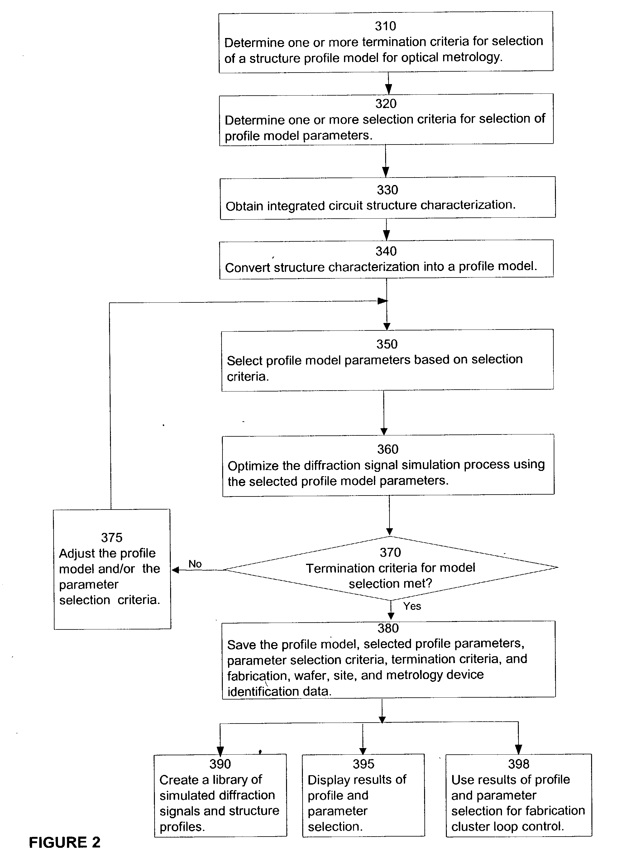
Model and parameter selection for optical metrology
a technology of optical metrology and model, applied in the field of integrated circuit (ic) metrology, can solve the problems of time-consuming and expensive empirical scatterometry technique for building a library, increasing the difficulty of measuring the features of ic devices, and prone to damag
- Summary
- Abstract
- Description
- Claims
- Application Information
AI Technical Summary
Benefits of technology
Problems solved by technology
Method used
Image

Examples
Embodiment Construction
)
[0036] In order to facilitate the description of the present invention, either an ellipsometric or reflectometric optical metrology system is used to illustrate certain concepts and principles. Graphs of diffraction signals off wafer structures using an ellipsometer, e.g., cos (.DELTA.) and tan (.PSI.), will be utilized to describe certain exemplary embodiments while reflectometric reflectance graphs will be utilized to describe others. It is understood that the same concepts and principles equally apply to ellipsometric, reflectometric, or other optical metrology systems.
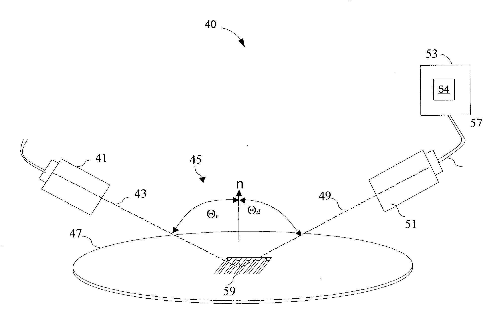
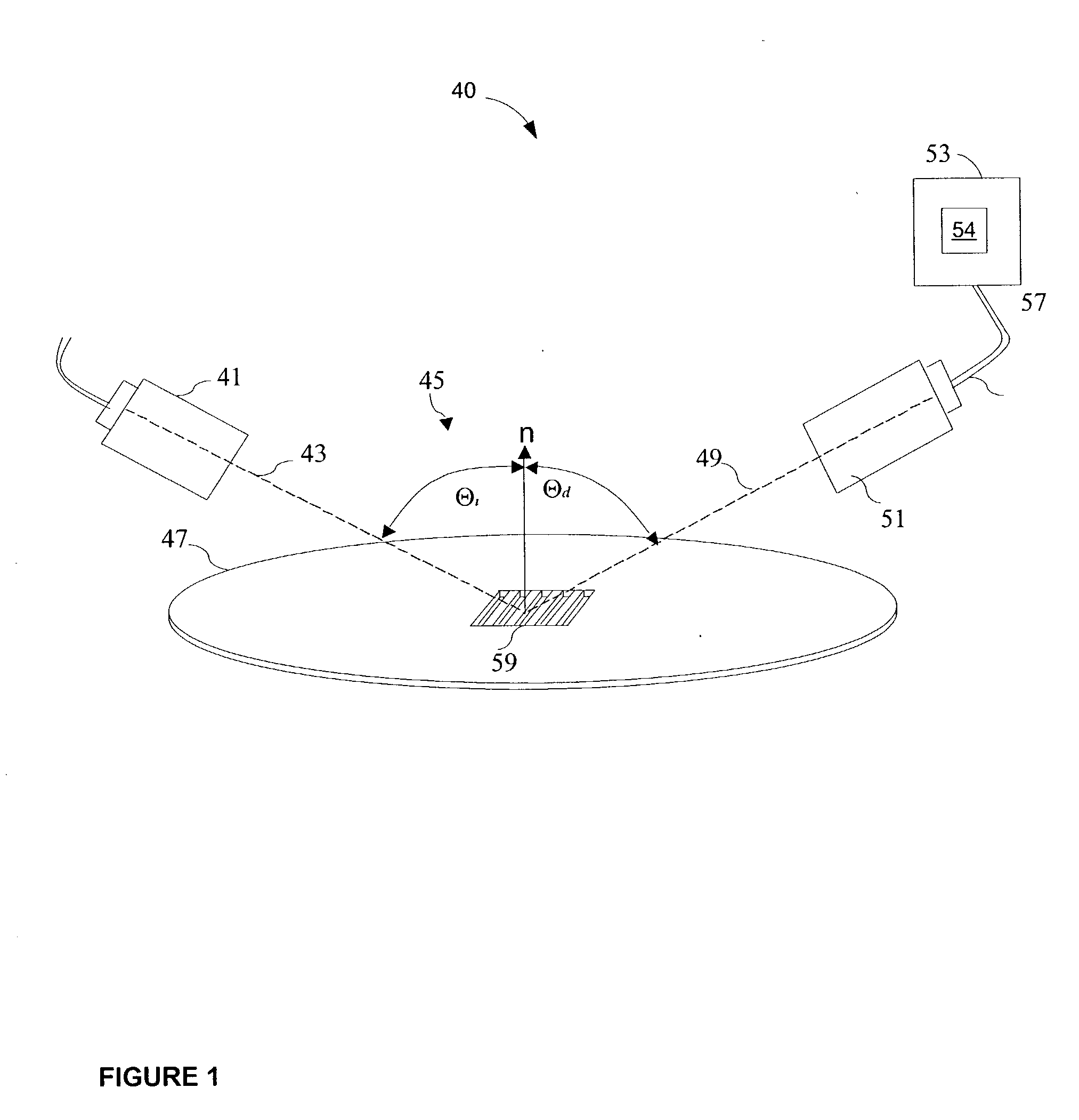
[0037] FIG. 1 is an architectural diagram illustrating the use of optical metrology to measure the diffraction signals off structures patterned on a wafer. The optical metrology system 40 includes a metrology beam source 41 projecting a beam 43 at the target structure 59 of a wafer 47. The metrology beam 43 is projected at an incidence angle .theta..sub.1 towards the target structure 59 and diffracted at a diffrac...
PUM
| Property | Measurement | Unit |
|---|---|---|
| thickness | aaaaa | aaaaa |
| thickness | aaaaa | aaaaa |
| width | aaaaa | aaaaa |
Abstract
Description
Claims
Application Information