Printed product incorporating inorganic semiconductors

a technology of inorganic semiconductors and printed products, which is applied in the field of printed products incorporating inorganic semiconductors to achieve the effect of increasing the speed of the substrate and increasing the speed

Active Publication Date: 2004-07-29
3D SYST INC
View PDF11 Cites 91 Cited by
  • Summary
  • Abstract
  • Description
  • Claims
  • Application Information

AI Technical Summary

Benefits of technology

[0015] In the preferred embodiments the printheads extend across the width of the substrate and are capable of printing across the full substrate width simultaneously i.e. they do not scan or raster when printing but are stationary. This enables a substrate to be moved past the printheads at a substantially constant speed, with the printheads printing rows of material onto the substrate. The substrate speed is matched to the row width and printhead cycle time so that the substrate has moved the width of the rows printed for each printhead cycle. Thus the next row or rows printed by each printhead will be printed next to a previously printed row or rows. In the preferred embodiments the printheads each print two rows simultaneously for increased substrate speed.
[0021] It will be appreciated that for production efficiency more than one printhead in a layer group may print the same material. Where the refill rate of the printheads for different materials is substantially the same, speed increases can only be achieved when all materials have the same number of printheads. However if one material requires a much longer refill time, provision of two or more printheads for that material alone may allow increased substrate speed.
[0041] At a substrate speed of 208 mm per second a typical production line can produce approximately 4.32 products per second, 373151 products per day or 136 million products per year, assuming the system runs continuously. Whilst this is greater than the current market for such products, the system has the potential to substantially reduce the cost of these products and so increase the market.
[0044] A flat panel TV of 53 cm diagonal size is generally the largest object that can be printed in the typical system. Of course to print wider objects, wider printheads may be utilized. For longer objects, more memory is required and for thicker objects the voxel height maybe increased or more layers printed by providing more layer groups. Whilst the printheads have the ability to vary the droplet size slightly, generally if a larger voxel size were required, different printheads would be required. Of course increased voxel size results in a higher `roughness` of the finished product. However, depending on the product, this may be commercially acceptable.
[0073] Preferably the reconfiguration is made with no loss of printed product.

Problems solved by technology

However, these systems typically utilize a single scanning printhead and are only useful for producing non-working models.

Method used


Image

  • Printed product incorporating inorganic semiconductors
  • Printed product incorporating inorganic semiconductors
  • Printed product incorporating inorganic semiconductors

Examples


Embodiment Construction

[0147] Basic Concept

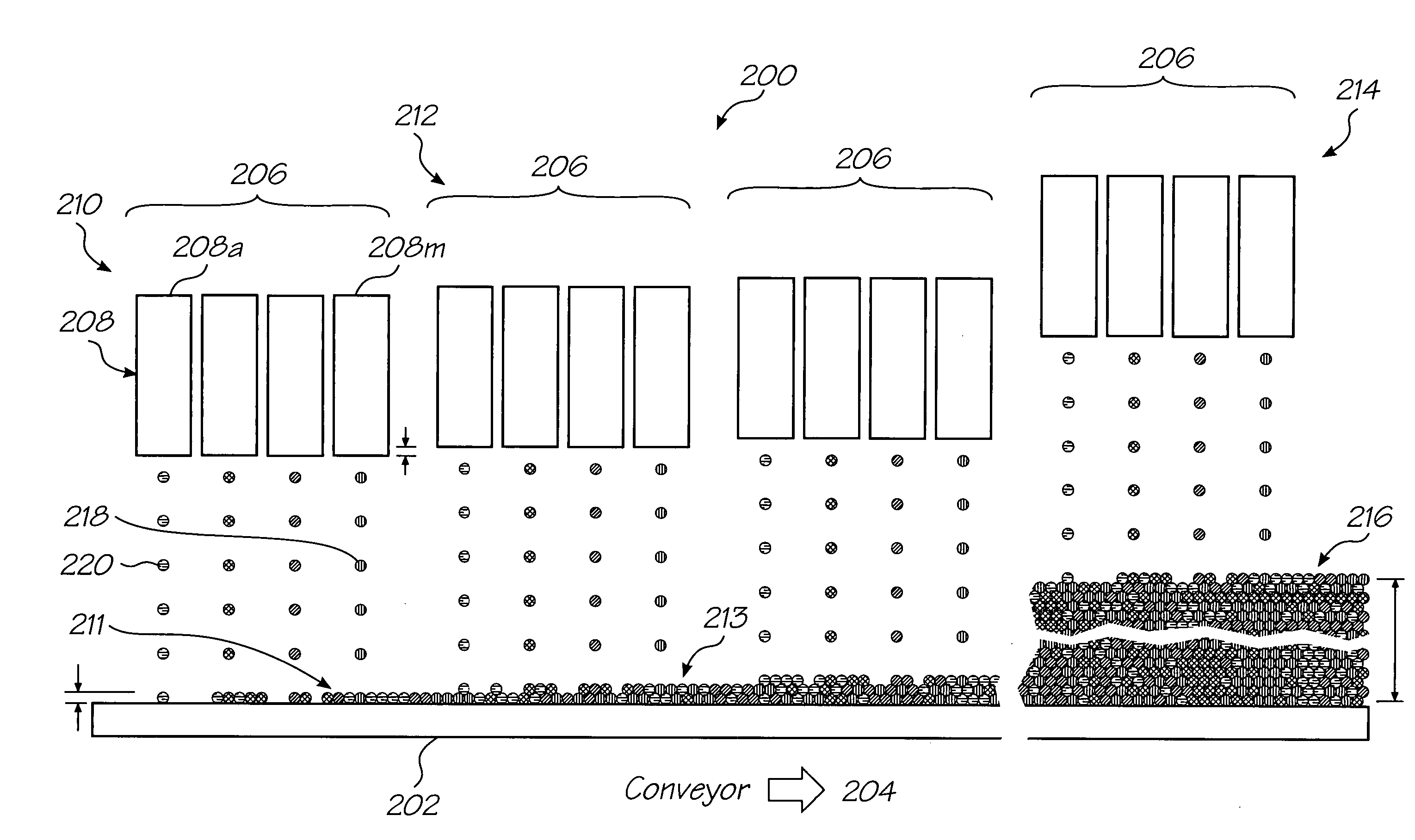
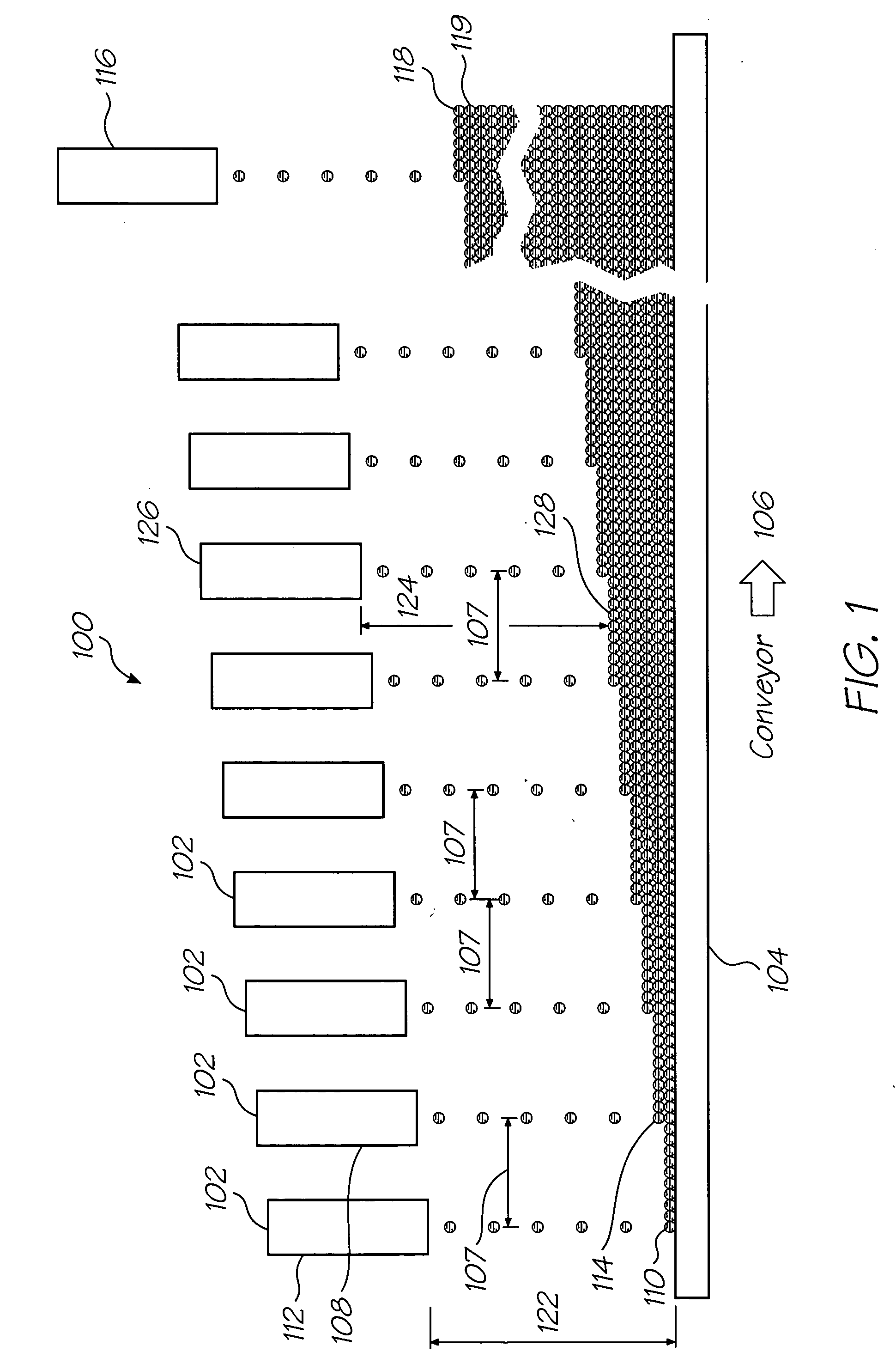
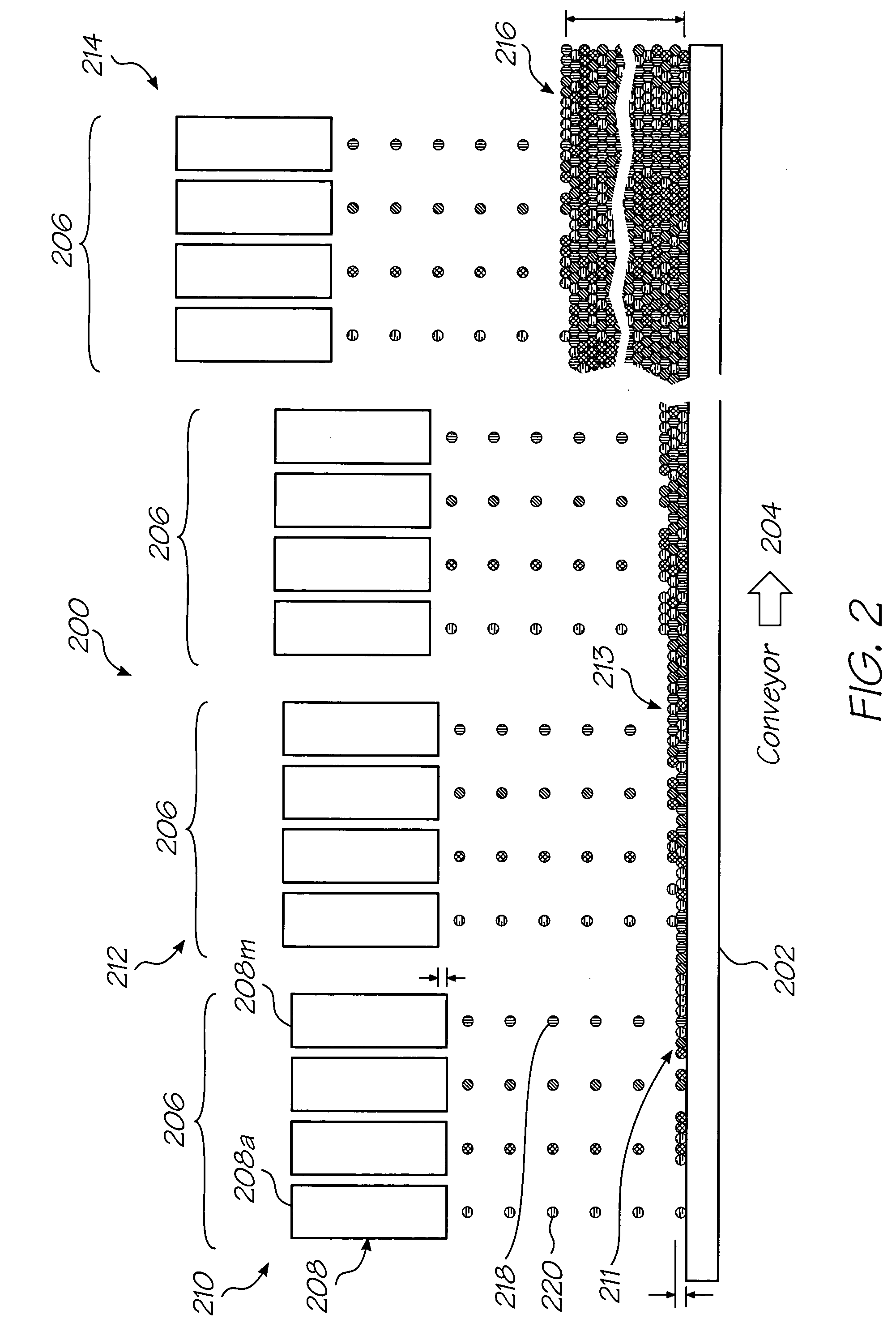
[0148] FIG. 1 schematically shows a simplified production line 100 having many substrate width printheads 102. The printheads 102 print materials onto a moving substrate 104, that is preferably moved at a substantially constant speed in a flat plane, as indicated by arrow 106. The printheads 102 extend across the width of the substrate 104 perpendicular to the direction of travel of the substrate and are, preferably, spaced along the substrate 104 with substantially constant separations. However, as will be explained later, constant separation of the printheads is not critical.

[0149] The printheads 102 print one layer of an object onto the previously printed layer. Thus the printhead 112 prints the first layer 110, the second printhead 108 prints a second layer 114 onto the first layer 110 and the N.sup.th printhead 116 prints an N.sup.th layer 118 onto the (n-1).sup.th layer 119. For clarity only one printhead is shown for each layer but in practice there will b...


PUM

PropertyMeasurementUnit
viscositiesaaaaaaaaaa
widthaaaaaaaaaa
heightaaaaaaaaaa

Abstract

A printing system including at least one printhead for printing material to create a printed product, and an object incorporation device that incorporates inorganic semiconductors into the product being printed whilst the at least one printhead prints the product.

Description

[0001] This invention relates to the creation of objects using digital additive manufacturing and more particularly to creating working objects that may be electrically and / or mechanically active.CO-PENDING APPLICATIONS[0002] Various methods, systems and apparatus relating to the present invention are disclosed in the following co-pending applications filed by the applicant or assignee of the present invention simultaneously with the present application:[0003] DAM01S, DAM02US, DAM03US, DAM04US, DAM05US, DAM06US, DAM07US, DAM08US, DAM09US, DAM11US, DAM12US, DAM13US, DAM14US.[0004] The disclosures of these co-pending applications are incorporated herein by cross-reference. Each application is temporarily identified by its docket number. This will be replaced by the corresponding USSN when available.[0005] Digital additive manufacturing is a process by which an object is defined three dimensionally by a series of volume elements (hereinafter referred to as voxels). The object is then p...

Claims


Application Information

Patent Timeline
Patent Type & Authority Applications(United States)
IPC IPC(8): B29C67/00B29C70/68B41J2/01B41J3/407B41J3/54B41J11/00
CPCB22F3/008B29C67/0059B29C70/68B41J2/01Y10T29/49144B41J3/543B41J11/002Y10S439/901B05C5/0212B41J3/4073B29C64/112B33Y70/00B33Y30/00B33Y40/00B33Y80/00B33Y10/00H05K1/185H05K3/125H05K3/4664B22F10/10Y02P10/25B41J11/0021B41J11/0022B41J11/0024B41J11/00214B41J11/00216B22F12/53B22F12/70B22F12/20B33Y50/02B41J29/393
Inventor SILVERBROOK, KIA
Owner 3D SYST INC
Why Eureka
Try Eureka