Package structure of an image sensor module

a technology of image sensor and module, which is applied in the direction of basic electric elements, electrical equipment, semiconductor devices, etc., can solve the problems of increasing manufacturing costs, complicated manufacturing processes, and high manufacturing costs

Inactive Publication Date: 2004-12-16
PRO TECHOR INT
View PDF0 Cites 16 Cited by
  • Summary
  • Abstract
  • Description
  • Claims
  • Application Information

AI Technical Summary

Problems solved by technology

The above-mentioned package structure of the image sensor module has a lot of elements and has a lot of complicated manufacturing processes.
Moreover, since the substrate 10 is made of ceramic materia

Method used


Image

  • Package structure of an image sensor module
  • Package structure of an image sensor module
  • Package structure of an image sensor module

Examples


Embodiment Construction

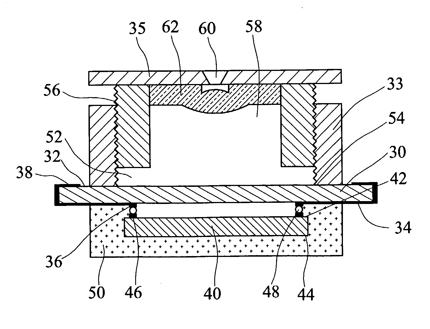
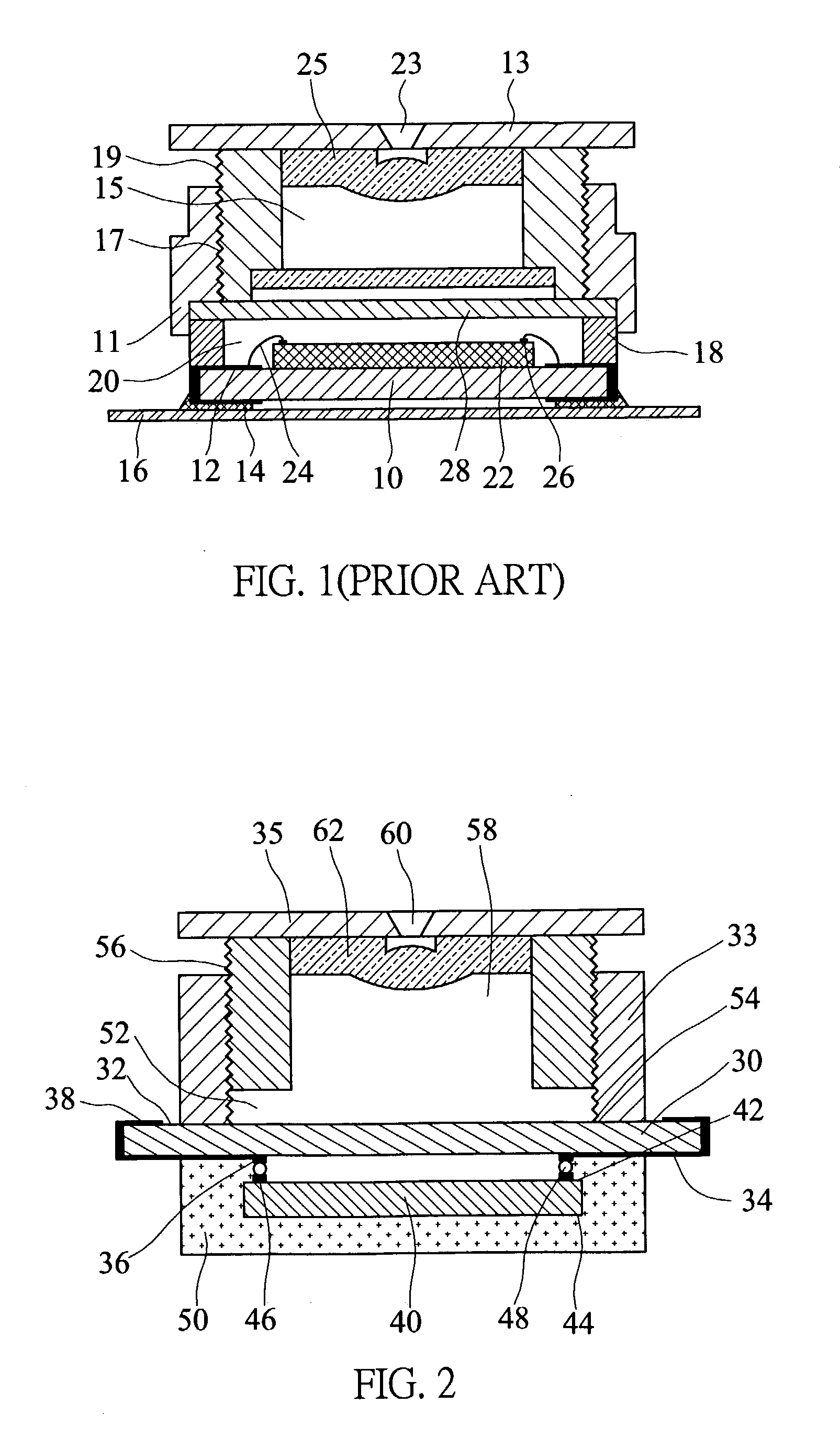
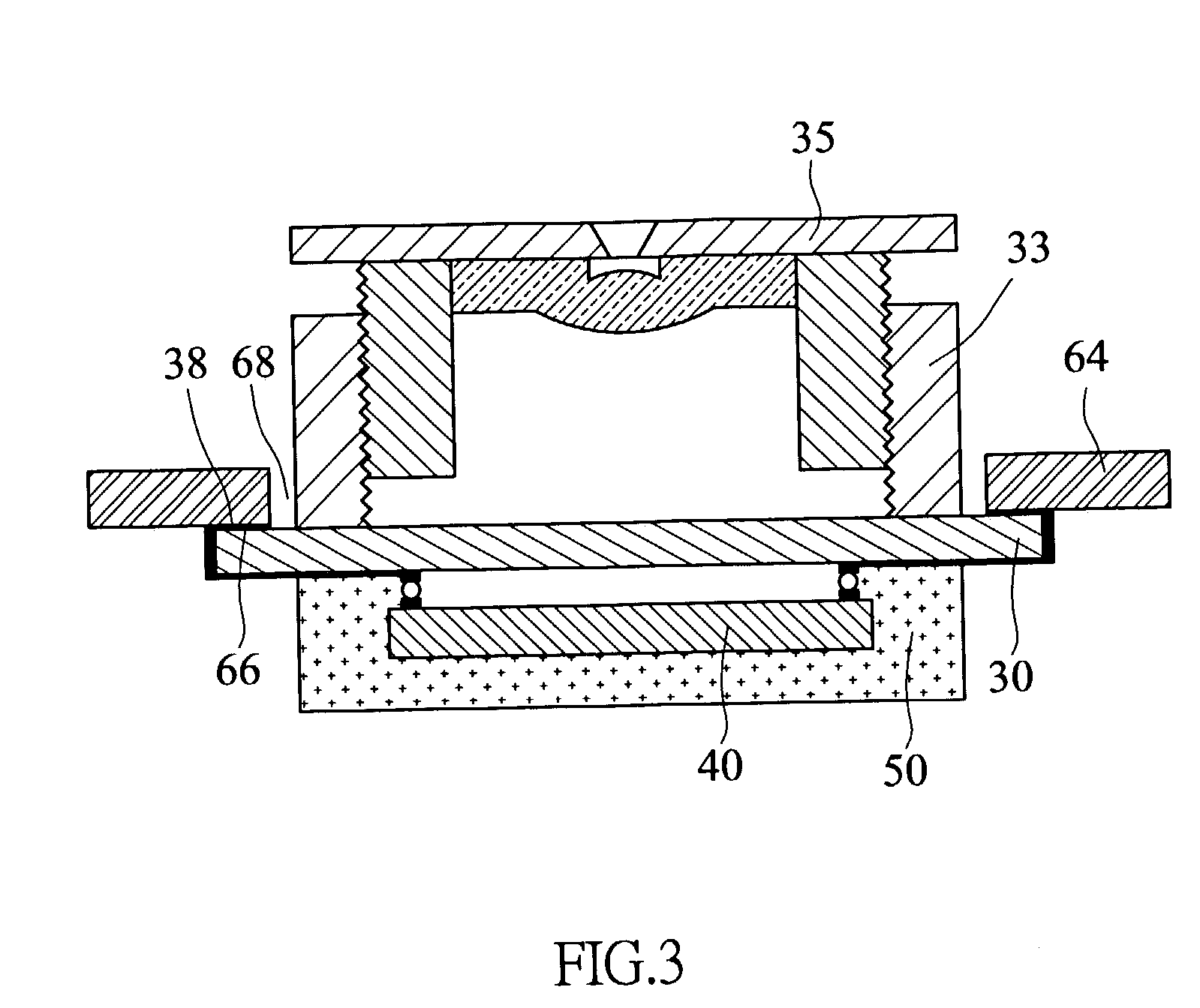
[0022] Referring to FIG. 2, a package structure of an image sensor module of the present invention includes a transparent layer 30, an image sensing chip 40, a lens holder33, a lens barrel 35 and a glue layer 50.

[0023] The transparent layer 30 may be a transparent glass, which has an upper surface 32 and a lower surface 34. A plurality of signal input terminals 36 are formed on the lower surface 34 by way of wire plating. Also, a plurality of signal output terminals 38 are formed on the upper surface 32. The signal input terminals 36 extend from the periphery of the lower surface 34 of the transparent layer 30 to the upper surface 32 so as to electrically connect to the signal output terminals 38.

[0024] The image sensing chip 40 has an first surface 42 and a second surface 44. Electrical circuits are formed on the upper surface 42. Each of the electrical circuits is formed with bonding pads 46 that are electrically connected to the transparent layer 30 by way of flip chip bonding. T...


PUM


Abstract

A package structure of an image sensor module for electrically connecting to a printed circuit board includes a transparent layer, an image sensing chip, a lens holder and a lens barrel. A plurality of signal input terminals and signal output terminals are formed on the transparent layer. The electrical circuits are formed on the image sensing chip, each of the electrical circuits is formed with bonding pads and is electrically connected to the transparent layer by way of flip chip bonding. A lens holder is formed with a through hole, an internal thread is formed on an inner wall of the through hole. The lens holder is mounted to the upper surface of the transparent layer. A lens barrel is arranged within the through hole of the lens holder and is formed with an external thread, which is screwed to the internal thread of the lens holder, the lens barrel is formed with a chamber and an opening communicating with the chamber.

Description

[0001] 1. Field of the Invention[0002] The present invention relates to a package structure of an image sensor module, in particular, to a package structure of an image sensor module, which is formed by way of flip chip bonding and capable of simplifying the manufacturing processes and lowering the manufacturing costs.[0003] 2. Description of the Related Art[0004] A general sensor is used for sensing signals, which may be optical or audio signals. The sensor of the invention is used for receiving image signals and transforming the image signals into electrical signals, which are transmitted to a printed circuit board.[0005] Referring to FIG. 1, a conventional image sensor module includes a substrate 10, a spacer 18, an image sensing chip 22, a transparent glass 28, a lens holder11 and a lens barrel13.[0006] The substrate 10 is made of ceramic materials. A plurality of signal input terminals 12 and signal output terminals 14 are formed on the periphery of the substrate 10. The signal...

Claims


Application Information

Patent Timeline
IPC IPC(8): H01L31/0203H01L31/0232
CPCH01L31/0203H01L31/0232H01L31/02325H01L2224/05568H01L2224/05573H01L2224/16225H01L2224/48091H01L2924/00014H01L2224/05599
Inventor YOU, IRVINGTU, HSIU WENWU, JICHENCHANG, JASONHSIEH, FIGO
Owner PRO TECHOR INT
Why Eureka
Try Eureka