Method of manufacturing solar cell

a manufacturing method and solar cell technology, applied in sustainable manufacturing/processing, climate sustainability, semiconductor devices, etc., can solve the problems of increasing the manufacturing cost increasing the defective rate of the solar cell, and the operation error of the semiconductor equipment, so as to reduce the defective rate of the edge isolation structure, reduce the contamination of semiconductor equipment, and simplify the manufacturing process

Active Publication Date: 2020-07-09
SHANGRAO JINKO SOLAR TECH DEV CO LTD
View PDF0 Cites 2 Cited by
  • Summary
  • Abstract
  • Description
  • Claims
  • Application Information

AI Technical Summary

Benefits of technology

[0049]According to the method of forming an isolation line by etching a portion of the semiconductor substrate by applying an etching paste to the edge of one surface or the other surface of the semiconductor substrate, contamination of semiconductor equipment may be minimized, and since the etching paste is applied to each solar cell, a defective rate for the edge isolation structure may be minimized.
[0050]In addition, since the edge isolation structure is formed by performing etching by applying the etching paste, a manufacturing process may be simplified.

Problems solved by technology

The sulfur hexafluoride (SF6), chlorine (Cl2), oxygen (O2), and the like remaining on the surface of the semiconductor substrate contaminate an outer wall of semiconductor equipment during transfer of the semiconductor substrate, resulting in an operation error of the semiconductor equipment.
In order to prevent the above problems, a separate additional auxiliary device should be installed in the semiconductor device, thereby increasing a manufacturing cost of the solar cell.
In addition, in the case of forming isolation using the RIE, isolation is formed on each semiconductor substrate in a state where a plurality of semiconductor substrates are arranged in a tray, and here, isolation is not formed as much as desired on the semiconductor substrate arranged on an outer portion of the tray, among the plurality of semiconductor substrates arranged in the tray, thereby increasing a defective rate of the solar cell and increasing the cost.

Method used


Image

  • Method of manufacturing solar cell
  • Method of manufacturing solar cell
  • Method of manufacturing solar cell

Examples


first embodiment

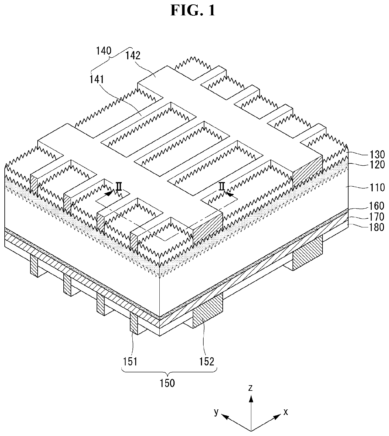
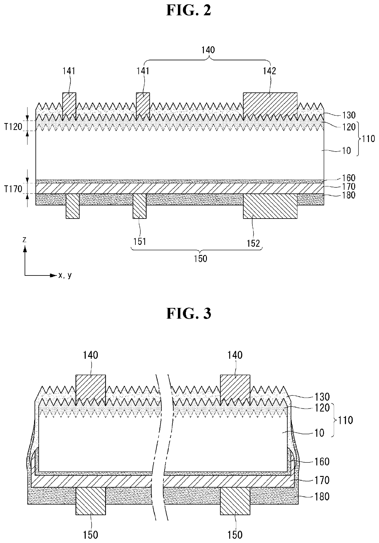
[0115]FIG. 3 is a view illustrating an isolation structure of a solar cell according to the present disclosure.

[0116]FIG. 3 illustrates a side surface of a solar cell in order to explain an isolation structure formed on the side surface of the solar cell illustrated in FIGS. 1 and 2.

[0117]As illustrated in FIG. 3, in the solar cell according to the present disclosure, the first conductive region and the second conductive region may be spaced apart from each other on the side surface of the semiconductor substrate to form an isolation structure.

[0118]More specifically, the first conductive region may be formed on the side surface of the semiconductor substrate and mainly formed on the back surface of the semiconductor substrate with respect to the center of the side surface of the semiconductor substrate (i.e., the center of the semiconductor substrate in the thickness direction) and the second conductive region may be mainly formed on the front surface of the semiconductor substrate...

second embodiment

[0199]The solar cell having an isolation structure has the same basic configuration as the solar cell illustrated in FIGS. 1 and 2, but there are some differences in positions of formation of each layer or film. In the following description, “A” is indicated after the numeral reference indicating each element.

[0200]Accordingly, elements having the same number in the drawings illustrating the isolation structure of the solar cell according to the first embodiment described above and in the drawings illustrating the isolation structure of the solar cell according to the second embodiment below may be regarded as the same elements having the same function.

[0201]FIG. 23 is a view illustrating an isolation structure of a solar cell according to the second embodiment of the present disclosure, and FIG. 24 is a cross-sectional view of an isolation line 200 illustrated in FIG. 23, taken along line II-II of FIG. 23. (a) of FIG. 23 shows the entire pattern of any one of one surface or the ot...


PUM

PropertyMeasurementUnit
thicknessaaaaaaaaaa
thicknessaaaaaaaaaa
thicknessaaaaaaaaaa

Abstract

Provided are a method of manufacturing a solar cell, including a polycrystalline silicon layer forming operation of forming a polycrystalline silicon layer containing a first dopant on a back surface of a semiconductor substrate formed of a single crystal silicon material including a base region, a front texturing operation of texturing a front surface of the semiconductor substrate and simultaneously removing the polycrystalline silicon layer formed on the front surface of the semiconductor substrate, a second conductive region forming operation of forming a second conductive region by diffusing a second dopant on the front surface of the semiconductor substrate, a passivation layer forming operation of forming a first passivation layer on the polycrystalline silicon layer formed on the back surface of the semiconductor substrate and forming a second passivation layer on the second conductive region of the front surface of the semiconductor substrate, and an electrode forming operation of forming a first electrode connected to the polycrystalline silicon layer through the first passivation layer and forming a second electrode layer at the second conductive region through the second passivation layer.

Description

CROSS-REFERENCE TO RELATED APPLICATION[0001]This application claims priority to and the benefit of Korean Patent Application No. 10-2019-0002792 filed in the Korean Intellectual Property Office on Jan. 9, 2019 and Korean Patent Application No. 10-2019-0007668 filed in the Korean Intellectual Property Office on Jan. 21, 2019, all of these applications are hereby expressly incorporated by reference into the present application.BACKGROUND OF THE INVENTIONField of the Invention[0002]The present disclosure relates to a solar cell manufacturing method, and more particularly, to a method of manufacturing a solar cell capable of simplifying a process of manufacturing a solar cell by isolating a first conductive region and a second conductive region when a front surface of a semiconductor substrate is textured during the solar cell manufacturing process.Related Art[0003]A solar cell includes an n-type conductive region and a p-type conductive region and may produce electric power as a carrie...

Claims


Application Information

Patent Timeline
Patent Type & Authority Applications(United States)
IPC IPC(8): H01L31/18H01L31/0747H01L31/0224H01L31/0216H01L31/0236
CPCH01L31/02168H01L31/02363H01L31/182H01L31/0747H01L31/022425H01L31/1804H01L31/0745H01L31/02167Y02E10/546Y02E10/547Y02P70/50
Inventor CHANG, WON JAEDO, YOUNG GUKIM, SUNG JINCHEONG, JU HWAAHN, JUN YONGCHO, HAE JONGKO, JI SOO
Owner SHANGRAO JINKO SOLAR TECH DEV CO LTD
Why Eureka
Try Eureka