Control circuit for error checking and correction and memory controller

a control circuit and memory controller technology, applied in error detection/correction, redundant data error correction, instruments, etc., can solve the problems of long time and complicated inverter, and achieve the effect of improving the accuracy of the test results

Inactive Publication Date: 2004-12-16
KK TOSHIBA
View PDF5 Cites 62 Cited by
  • Summary
  • Abstract
  • Description
  • Claims
  • Application Information

AI Technical Summary

Problems solved by technology

However, because this document does not consider the property of the ECC code, the inverter becomes complicated as bit to be inverted by the bit inverter is not fixed.
However, a complicated inverter has a number of test items and takes a long time to make a test.

Method used


Image

  • Control circuit for error checking and correction and memory controller
  • Control circuit for error checking and correction and memory controller
  • Control circuit for error checking and correction and memory controller

Examples


first embodiment

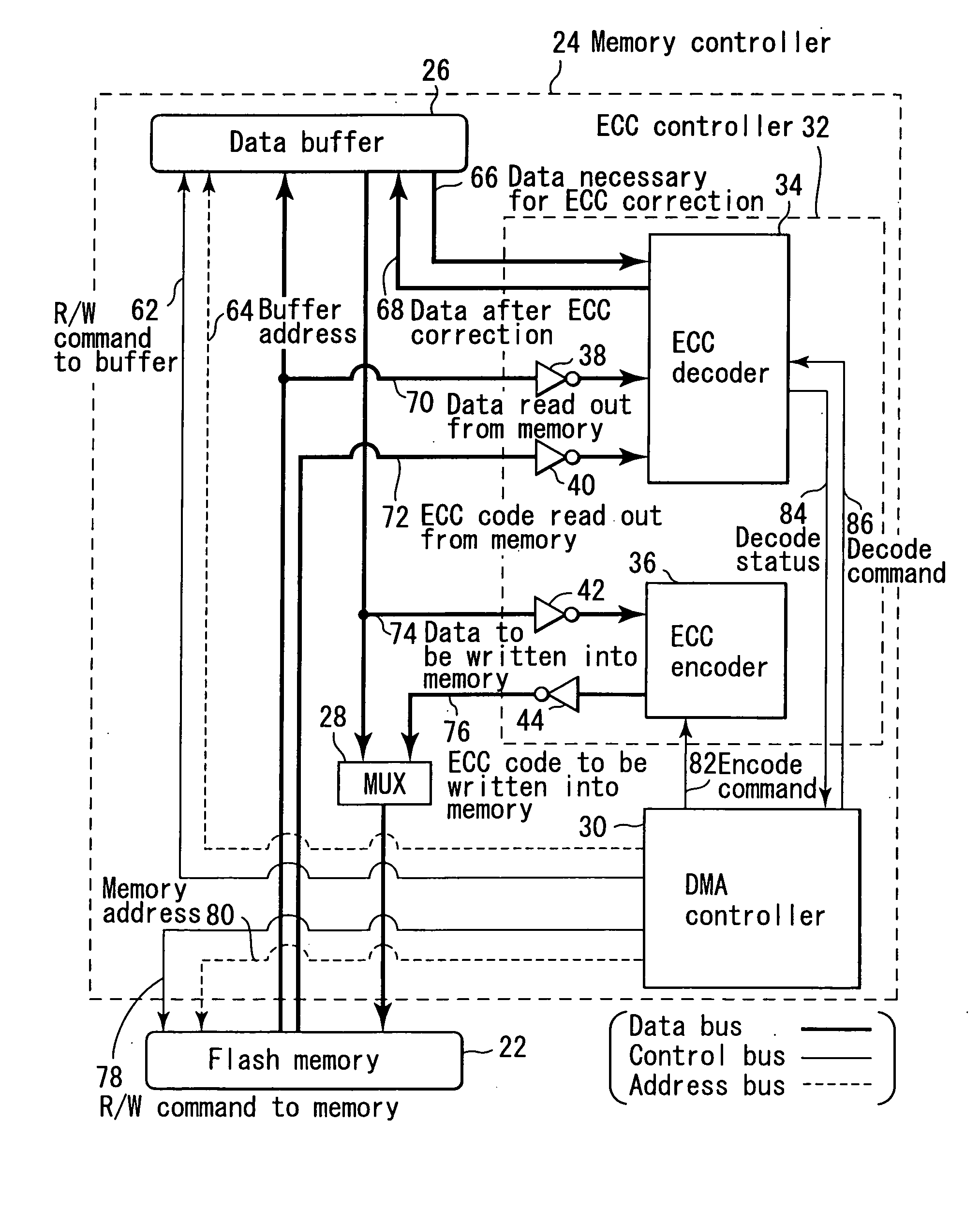
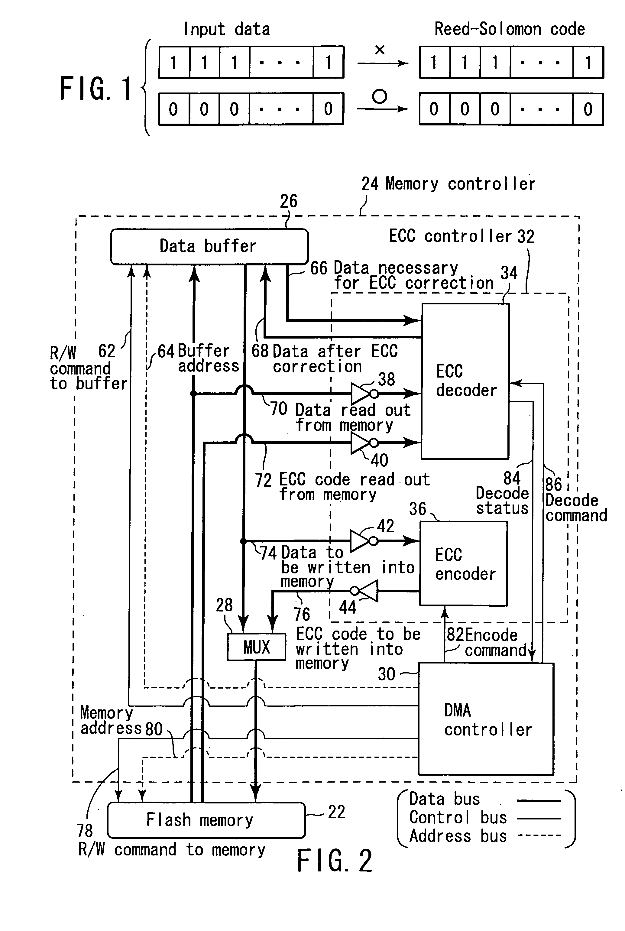
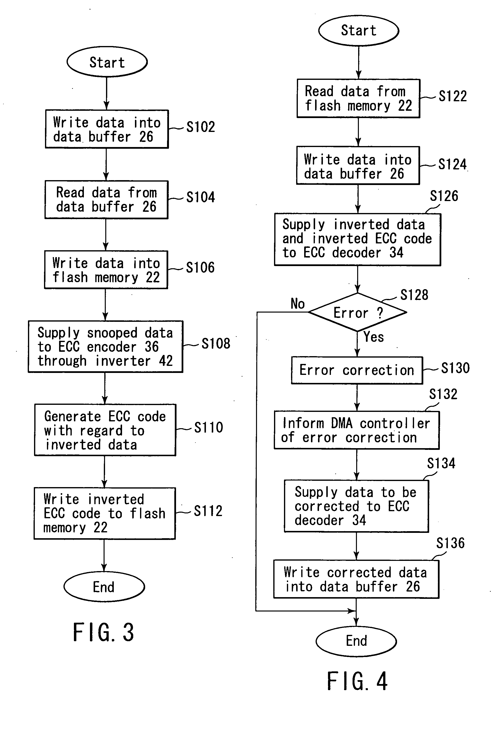
[0043] FIG. 2 is a diagram showing the entire configuration of a system including an ECC circuit according to the present invention. According to this embodiment, an inverter is connected to a data bus and an ECC code bus such that any ECC error is not detected from the initial value after erasure.

[0044] A memory controller 24 is connected to a flash memory 22 through a data bus, a control bus and an address bus. The memory controller 24 comprises a data buffer 26, a multiplexer 28, a DMA controller 30, and an ECC controller 32. The data buffer 26 temporarily holds write data to be written into the flash memory 22 and read data to be read out from the flash memory 22. The ECC controller 32 executes ECC coding processing for the write data and ECC decoding processing for the read data. The multiplexer 28 selectively supplies data from the data buffer 26 and data from the ECC controller 32 to the flash memory 22. The DMA controller 30 supplies address data and control data to the flas...

second embodiment

[0064] Although according to the first embodiment shown in FIG. 2, the ECC control is performed by the DMA controller 30, that control can be carried out by using a CPU instead of the DMA controller 30 also. FIG. 5 is a block diagram of the second embodiment which achieves this. That is, a CPU 50 is provided instead of the DMA controller 30. A ROM module 52 which stores a program for actuating the CPU 50 and a RAM module 54 serving as a working region for the CPU 50 are provided. Following two controls are different as compared to a case where the DMA controller 30 carries out the ECC control.

[0065] (1) Before carrying out the ECC control, the CPU 50 loads a program from the ROM module 52 through a program read data line 92.

[0066] (2) When the ECC control is carried out, the CPU 50 uses the RAM module 54 as a working region through a RAM access data line 94.

[0067] The other control is the same as the first embodiment.

[0068] As described above, the second embodiment can provide the s...


PUM


Abstract

A control circuit for a memory device, comprises an inverter which inverts all bits of data read out from the memory device, and a decoder which executes error correction and decoding for an output of the inverter.

Description

[0001] This application is based upon and claims the benefit of priority from the prior Japanese Patent Application No. 2003-024861, filed Jan. 31, 2003, the entire contents of which are incorporated herein by reference.[0002] 1. Field of the Invention[0003] The present invention relates to a control circuit and a memory controller for error checking and correction (hereinafter referred to as ECC) in a semiconductor memory device or the like.[0004] 2. Description of the Related Art[0005] There is a flash memory as an example of a nonvolatile semiconductor memory device. For example, in a NAND type flash memory, writing is carried out in each block of 512 bytes. In some type, the writing is executed while write address is increased continuously although the block is permitted to be discontinuous. If it is intended to write data in an intermediate block (smaller address) after it is written into discontinuous multiple blocks temporarily, it is necessary to transfer the data written in...

Claims


Application Information

Patent Timeline
Patent Type & Authority Applications(United States)
IPC IPC(8): G06F11/08G06F11/10G06F12/16G11C29/02
CPCG06F11/1068G11C29/02
Inventor TAKAI, YORIHARU
Owner KK TOSHIBA
Why Eureka
Try Eureka