Apparatus for inspection of a wafer

a technology for wafers and apparatuses, applied in the field of apparatus for inspection of wafers, can solve the problems of insufficient assessment of the edge profile of features configured on the wafers, insufficient contrast of the above-mentioned types of illumination, etc., and achieve the effect of simple and high contras

Active Publication Date: 2005-01-06
VISTEC SEMICON SYST
View PDF9 Cites 25 Cited by
  • Summary
  • Abstract
  • Description
  • Claims
  • Application Information

AI Technical Summary

Benefits of technology

[0007] It is the object of the present invention to create an apparatus for inspection of a wafer with which macrodefects can be determined with high contrast. A further intention is to create an apparatus for inspection of a wafer with which the quality of the edge profile of features configured on the wafer can be assessed reliably and in simple fashion.
[0017] To make the design of the apparatus even more flexible, the incidence angle α of the illuminating light beam can also be modified, a region on the surface of the wafer illuminated by the incident illuminating light beam preferably remaining stationary upon modification of the incidence angle so that, advantageously, the orientation of the image capture device does not need to be modified. Modification of the incidence angle α thus allows defects on the surface of the wafer to be identified and evaluated under different illumination conditions. Changing the incidence angle α makes it possible, in particular, to assess the quality of the edge profile of features configured on the wafer, and of defects present at edges, in advantageously simple fashion. At a certain incidence angle α, for example, right-angle edges may ideally result in a relative low scattered-light intensity, whereas rounded edges deviating from the ideal right-angle shape may result only in an elevated scattered-light intensity or even in a directly reflected or diffracted light component, which is detected by the image capture device.
[0025] The imaging optical system is preferably designed also to make possible a certain spatial separation between illumination system, imaging components, and image capture elements. According to a first embodiment, the imaging optical system encompasses a respective mirror in order to deflect the respective illuminating light beam in a different direction. Preferably, an oblique or raking incidence of the illuminating light beam is thereby implemented with no need to arrange imaging optical elements in the immediate vicinity of the wafer to be inspected. By means of suitable imaging optical elements arranged in the beam path of the illuminating light beam, the illuminating light beam can be shaped in such a way that an even more homogeneous illumination can be implemented. According to this embodiment, the incident-light illumination device can be aligned, in particular, perpendicular to the surface of the wafer, so that the base area of the apparatus according to the present invention can be reduced even further.
[0026] According to another embodiment, the imaging optical system encompasses in each case a periscope arrangement of mirrors having an inflected beam path in order to deflect a respective illuminating light beam in a different direction. The two mirrors of the periscope arrangement are preferably arranged parallel to one another and are pivotable and / or movable in coordination with one another, so that the incidence angle of the illuminating light beam incident onto the surface of the wafer can easily be modified. In this configuration the incident-light illumination device can also be oriented parallel to the surface of the wafer; this can offer advantages, for example, in terms of maintenance of the incident-light illumination device.
[0028] Preferably the wafer can be arranged below the separation panel, and the at least two incident-light illumination devices and / or the image capture device are arranged above the separation panel. In this configuration, the mirror arranged below the separation panel can be held in stationary fashion, and an alignment of the illuminating light beams can be brought about exclusively by adjusting optical elements arranged above the separation panel. It is advantageous that the apparatus according to the present invention can be aligned more easily and more reliably, and that even more favorable conditions can be created for the installation, maintenance, and operation of the apparatus.

Problems solved by technology

For certain macrodefects, the aforesaid types of illumination do not produce enough contrast.
In addition, the quality of the edge profile of features that are configured on the wafer, for example protrusions, conductor paths, etched depressions, or the like, cannot be adequately assessed.

Method used


Image

  • Apparatus for inspection of a wafer
  • Apparatus for inspection of a wafer
  • Apparatus for inspection of a wafer

Examples


Embodiment Construction

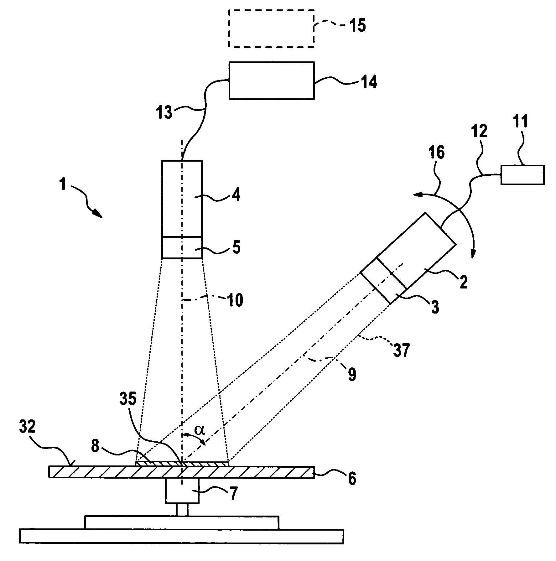
[0039]FIG. 1 shows, in a schematic cross section, a wafer inspection apparatus 1 according to the present invention. It encompasses an incident-light illumination device 2 that defines an illumination axis 9 which intersects surface 32 of wafer 6 at incidence point 35, a camera 4 serving as image capture device, and a wafer receiving device 7 that holds wafer 6 in either stationary or rotatable fashion. Wafer 6 is vacuum-suctioned onto wafer receiving device 7. Incident-light illumination device 2 comprises an imaging optical element 3, for example a lens or objective, that shapes illuminating light beam 37 in such a way that illuminating light beams 37, incident in inclined fashion onto surface 32 of wafer 6 to be inspected, illuminate a corresponding region 8 that covers the entire surface of wafer 6 or a subregion thereof, for example individual dies.

[0040] Camera 4 is perpendicular to surface 32 of wafer 6 and defines an imaging axis 10 that intersects surface 32 of wafer 6 at ...


PUM

PropertyMeasurementUnit
incidence angleaaaaaaaaaa

Abstract

The invention concerns an apparatus for inspection of a wafer, encompassing at least two incident-light illumination devices that radiate a respective illuminating light beam which is incident obliquely onto the surface of a wafer to be inspected and respectively defines an illumination axis, an image capture device for capturing an image of the surface in a dark-field arrangement, and a wafer receiving device for receiving the wafer, on whose surface linearly extending features are configured, in a definable orientation. The apparatus is characterized in that the illumination axes are oriented perpendicular to one another, and the apparatus is designed in such a way that a projection of the respective illumination axis onto the surface of the wafer is oriented substantially perpendicular to respective linear features on the surface of the wafer. With the apparatus, macrodefects can be detected and the quality of the edge profile of features configured on the surface of the wafer can be assessed.

Description

CROSS REFERENCE TO RELATED APPLICATIONS [0001] This application claims priority of the German patent application 103 30 006.6 which is incorporated by reference herein. FIELD OF THE INVENTION [0002] The present invention concerns an apparatus for inspection of a wafer, and concerns in particular an apparatus for the detection of macrodefects and for assessment of the edge profile of features, for example integrated circuits (ICs), that are configured on the wafer. BACKGROUND OF THE INVENTION [0003] In semiconductor production, wafers are processed sequentially in a plurality of process steps during the production process. With increasing integration density, requirements in terms of the quality of features to be configured on the wafer are rising. It is advantageous for this purpose if the quality even of individual process steps, for example lithography steps, can be dependably assessed during the production process and prior to a subsequent process step. The reason is that if a de...

Claims


Application Information

Patent Timeline
Patent Type & Authority Applications(United States)
IPC IPC(8): G01N21/88G01N21/95G01N21/956
CPCG01N21/8806G01N21/9501G01N2021/8822G01N21/956G01N21/9503
Inventor KREH, ALBERTBACKHAUSS, HENNING
Owner VISTEC SEMICON SYST
Why Eureka
Try Eureka