

Defect inspection apparatus
a technology of inspection apparatus and defect, applied in the direction of instruments, image analysis, image enhancement, etc., can solve the problems of contaminating objects, difficult to secure stable quality, and operators may miss detecting defects
- Summary
- Abstract
- Description
- Claims
- Application Information
AI Technical Summary
Benefits of technology
Problems solved by technology
Method used
Image

Examples
Embodiment Construction
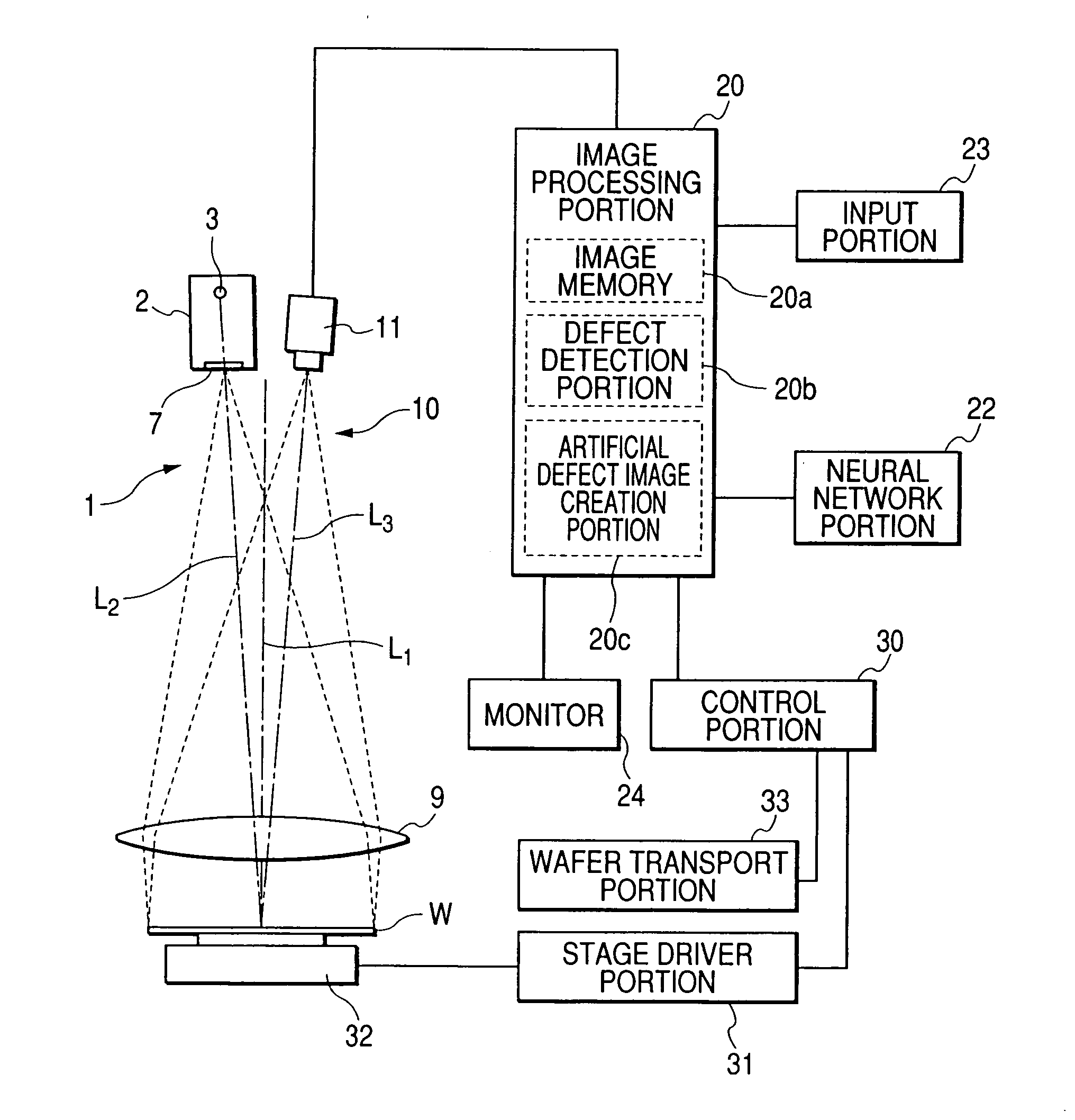
One embodiment of the present invention is hereinafter described with reference to the drawings. FIG. 1 is a schematic diagram of a defect inspection apparatus according to the present invention.
A stage 32 is moved in the X- and Y-directions (in directions parallel to the stage surface) by a stage moving portion 31. A wafer W that is an object to be inspected is automatically transported onto the stage 32 by a wafer transport portion 33 and placed on the stage 32 such that the inspected surface is placed on the top. A control portion 30 controls the whole of the inspection apparatus.
An illumination optical system 1 illuminates the surface (inspected surface) of the wafer W placed on the stage 32. The illumination optical system 1 includes an illumination unit 2 having a light source and a collimator lens 9 having a diameter larger than that of the wafer W. An imaging optical system 10 takes an image of the surface of the wafer W illuminated by the illumination optical system 1....
PUM
 Abstract
Description
Claims
Application Information