
Spin valve transistor with self-pinned antiparallel pinned layer structure

Inactive Publication Date: 2005-01-27
HITACHI GLOBAL STORAGE TECH NETHERLANDS BV
View PDF10 Cites 8 Cited by
  • Summary
  • Abstract
  • Description
  • Claims
  • Application Information

AI Technical Summary

Benefits of technology

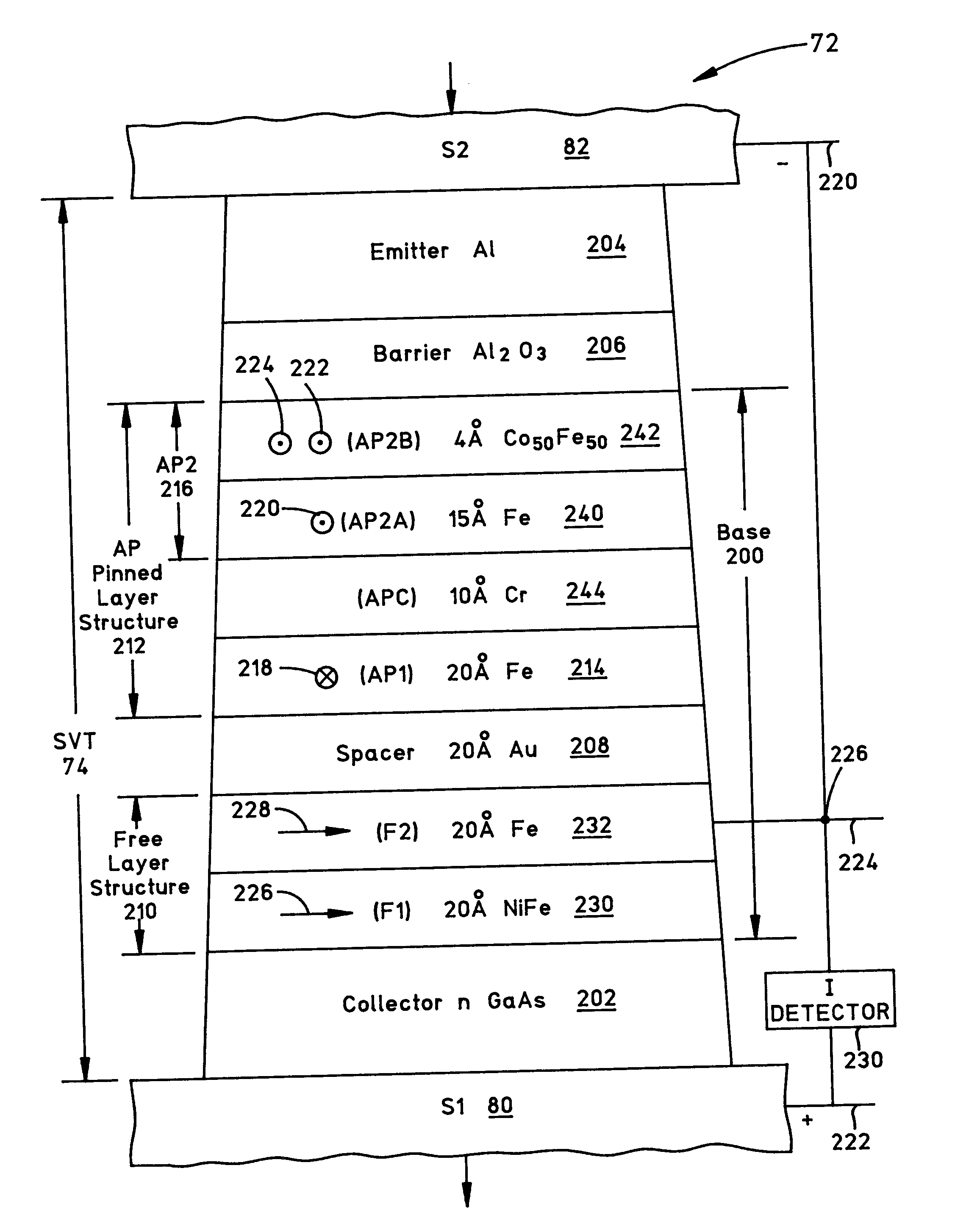
[0011] The present invention provides the base of the SVT with a pinned layer structure which is self-pinned so as to obviate the need of a pinning layer. By eliminating the pinning layer, which is typically thick in comparison to the other layers, scattering of the hot electrons is minimized and the transfer coefficient (IC/IE) is improved. The pinned layer structure is an antiparallel (AP) pinned layer structure which has first and second AP pinned layers which are separated by a thin antiparallel coupling layer. One of the AP pinned layers has a higher positive magnetostriction than the other AP pinned layer. During fabrication of the head assemblies the heads are lapped to a head surface which causes compressive stress within the AP pinned layers. Because of a positive magnetostriction in the one AP pinned layer it will have a magnetostrictive uniaxial anisotropy which is oriented perpendicular to the head surface. After fabrication of the head assembly a strong magnetic field is applied to orient a magnetization of the sensor either into or out of the head

Problems solved by technology

Unfortunately, a SVT can have a very low transfer coefficient which is the collector current to the emitter current (IC / IE).

Method used


Image

  • Spin valve transistor with self-pinned antiparallel pinned layer structure
  • Spin valve transistor with self-pinned antiparallel pinned layer structure
  • Spin valve transistor with self-pinned antiparallel pinned layer structure

Examples


Embodiment Construction

[0025] Magnetic Disk Drive

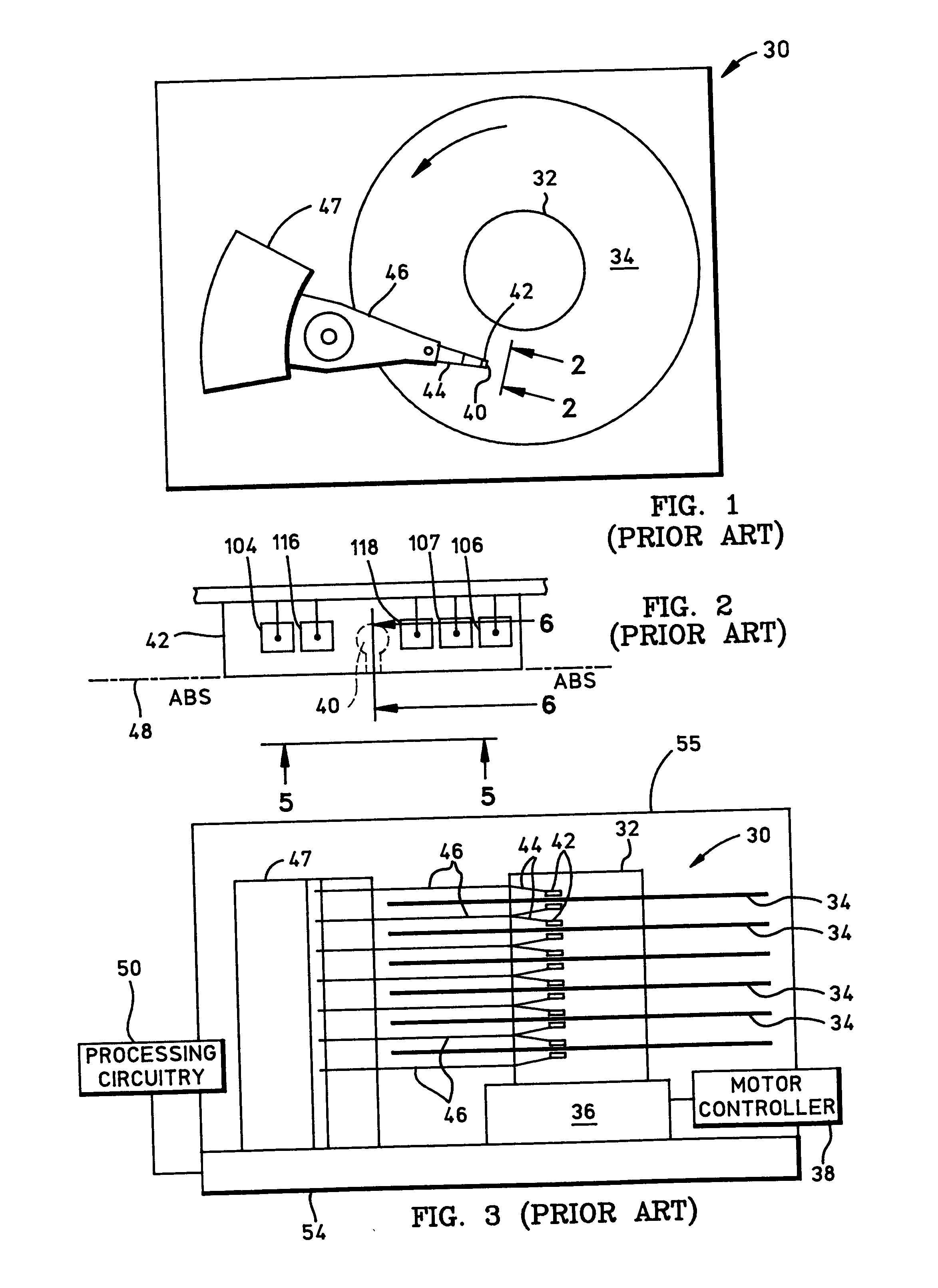
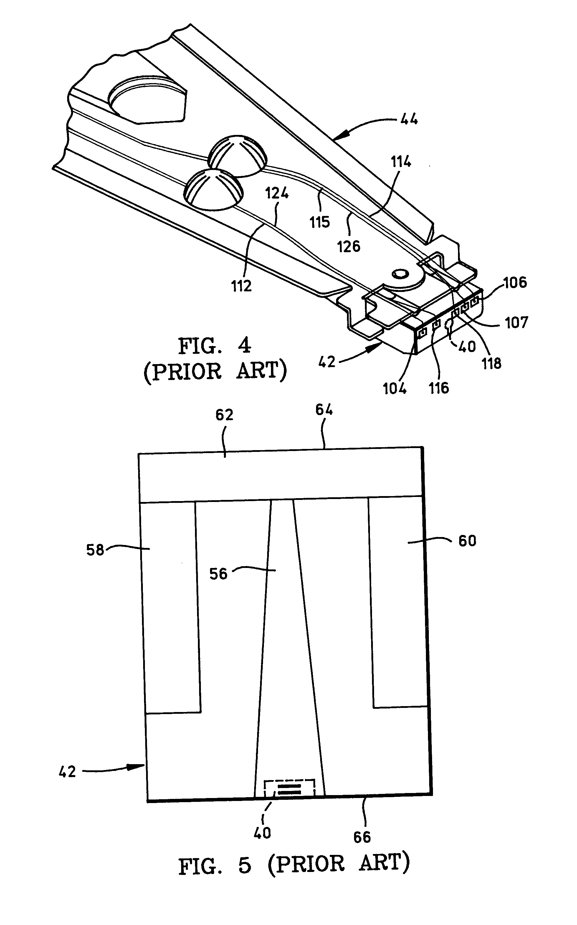
[0026] Referring now to the drawings wherein like reference numerals designate like or similar parts throughout the several views, FIGS. 1-3 illustrate a magnetic disk drive 30. The drive 30 includes a spindle 32 that supports and rotates one or more magnetic disks 34. The spindle 32 is rotated by a spindle motor 36 that is controlled by a motor controller 38. A slider 42 has a combined read and write magnetic head 40 and is supported by a suspension 44 and actuator arm 46 that is rotatably positioned by an actuator 47. A plurality of disks, sliders and suspensions may be employed in a large capacity direct access storage device (DASD) as shown in FIG. 3. The suspension 44 and actuator arm 46 are moved by the actuator 47 to position the slider 42 so that the magnetic head 40 is in a transducing relationship with a surface of the magnetic disk 34. When the disk 34 is rotated by the spindle motor 36 the slider is supported on a thin (typically, 0.01 μm) cush...


PUM


Abstract

A spin valve transistor includes an emitter, a collector, a base between the emitter and the collector, a spin valve which includes a free layer structure, a self-pinned antiparallel (AP) pinned layer structure and a nonmagnetic spacer layer between the free layer structure and the AP pinned layer structure wherein the base includes at least the free layer structure.

Description

BACKGROUND OF THE INVENTION [0001] 1. Field of the Invention [0002] The present invention relates to a spin valve transistor with a self-pinned antiparallel (AP) pinned layer structure wherein first and second AP pinned layers of the AP pinned layer structure comprise different materials for self-biasing the AP pinned layer structure. [0003] 2. Description of the Related Art [0004] The heart of a computer is a magnetic disk drive which includes a rotating magnetic disk, a slider that has read and write heads, a suspension arm above the rotating disk and an actuator arm that swings the suspension arm to place the read and write heads over selected circular tracks on the rotating disk. When the disk is not rotating the actuator arm parks the suspension arm and slider on a ramp. When the disk rotates and the slider is positioned by the actuator arm above the disk, air is swirled by the rotating disk adjacent an air bearing surface (ABS) of the slider causing the slider to ride on an ai...

Claims


Application Information

Patent Timeline
IPC IPC(8): G11B5/39H01F10/32H01L29/66H01L43/08
CPCB82Y10/00G11B5/3906H01F10/3272H01F10/329H01L43/08H01F10/3286H01L29/66984H10N50/10
Inventor GILL, HARDAYAL SINGH
Owner HITACHI GLOBAL STORAGE TECH NETHERLANDS BV
Learn More