
Method of generating an enable signal of a standard memory core and relative memory device

a technology of relative memory and enable signal, which is applied in the field of methods, can solve the problems of inability to form memory, inability to meet the needs of users, and increase the number of pins of the pins of the memory core,

Active Publication Date: 2005-02-10
MICRON TECH INC
View PDF8 Cites 18 Cited by
  • Summary
  • Abstract
  • Description
  • Claims
  • Application Information

AI Technical Summary

Problems solved by technology

Moreover, often the user must preliminary program the standard memory core of the device.
Because of the different requirements of specific serial communication protocols and of parallel communication protocols, it has not been possible so far to form memory devices that could be configured at fabrication level for supporting a Firmware Hub serial communication protocol or a different LPC serial communication protocol besides an SPI serial communication protocol and a parallel communication protocol of the type A / AMUX, without significantly increasing the number of pins.
However, an increase in the number of pins is often unacceptable or costly.

Method used


Image

  • Method of generating an enable signal of a standard memory core and relative memory device
  • Method of generating an enable signal of a standard memory core and relative memory device
  • Method of generating an enable signal of a standard memory core and relative memory device

Examples


Embodiment Construction

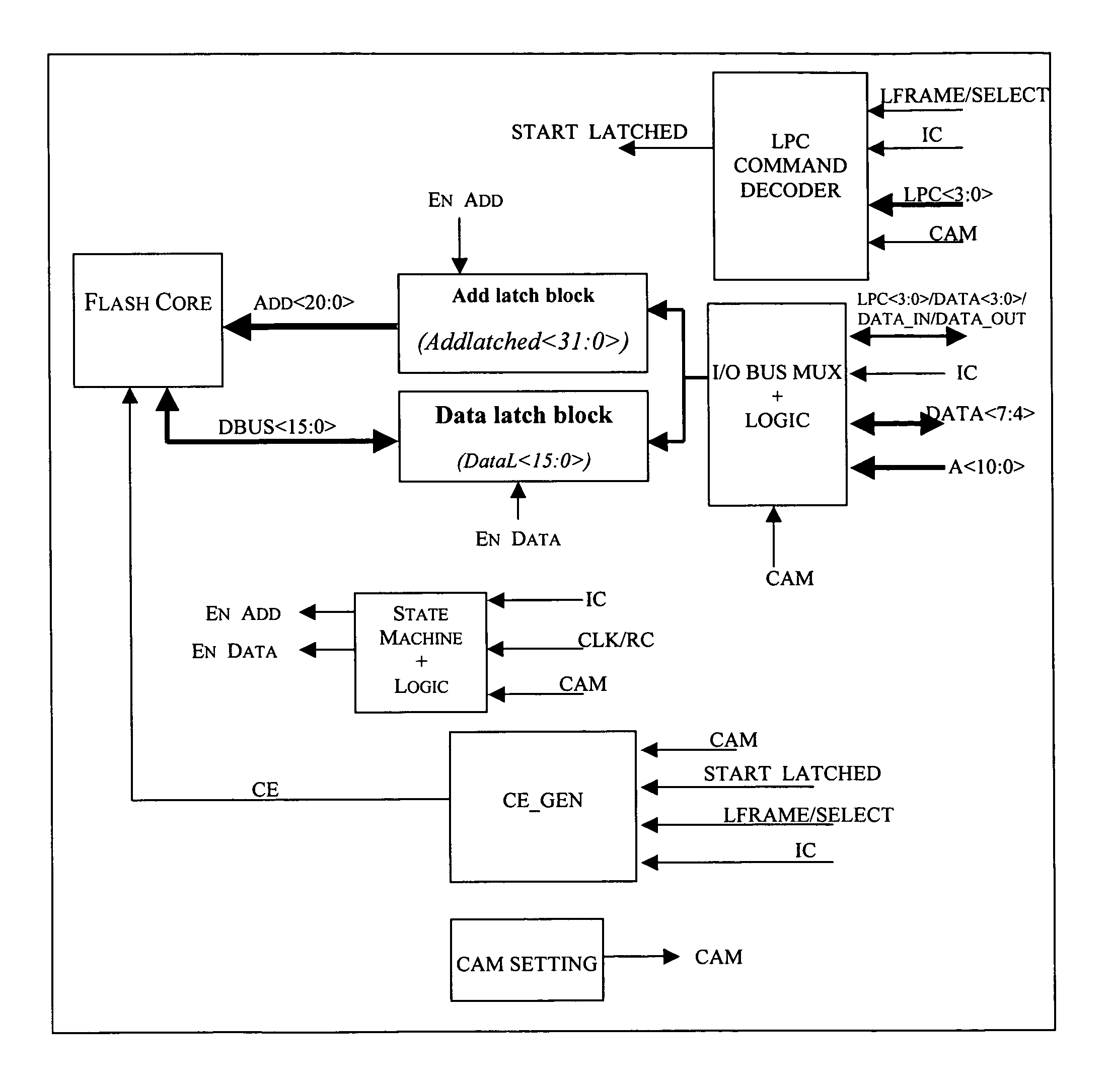
[0035] The memory device of the invention, depicted in FIG. 7, supports serial communication protocols LPC and SPI and a parallel communication protocol. The device contains a multi-protocol interface capable of communicating by using anyone of the supported protocols, and requires only an additional pin (LFRAME / SELECT) compared to a standard memory device accessed in parallel mode. This is achieved by exploiting the same pins for providing signals of different objects to the memory device depending on the communication protocol being used.

[0036] In the embodiment shown, the device of FIG. 7 is interfaced with an external data bus DATA7:0>, and to an external address bus A10:0>and has a first pin on which it receives an externally generated timing signal CLK (necessary for serial mode communications) or an address multiplexing signal RC (for parallel mode communications), a second pin on which it receives a start signal LFRAME / SELECT for either a serial communication protocol (LFRA...


PUM


Abstract

A memory device is configured for communicating with one of two different serial protocols, respectively an LPC or an SPI protocol, as well as with a parallel communication protocol through a multi-protocol interface while requiring only a single additional pin as compared to a standard memory device accessible with a parallel communication protocol. This result is achieved by exploiting the same pin for providing a timing signal for serial mode communications or an address multiplexing signal for parallel mode communications. The additional pin is used for conveying a start signal of an A / AMUX parallel communication protocol. The interface includes logic circuits that generate an enable signal for the standard memory core of the memory device.

Description

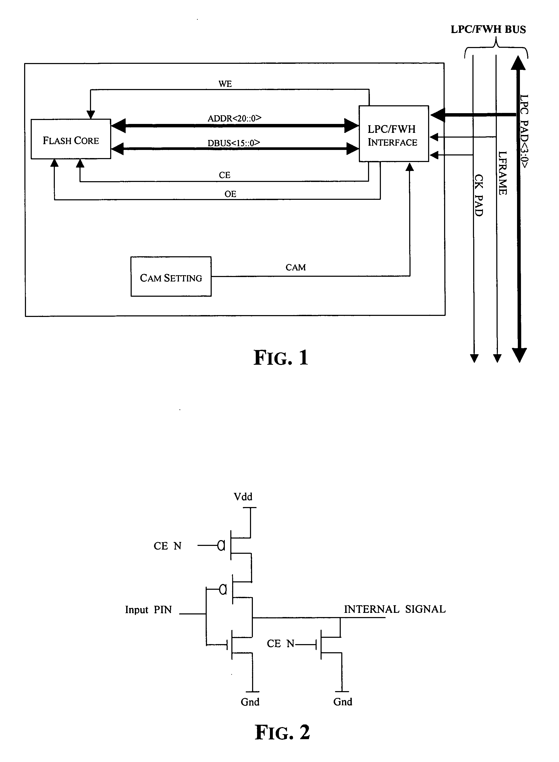
FIELD OF THE INVENTION [0001] The present invention relates in general to memory devices, and more particularly, to a memory device that supports different communication protocols by recognizing the protocol of the coded data. BACKGROUND OF THE INVENTION [0002] Volatile and non-volatile memory devices have a number of applications, such as in digital cameras and measuring instruments, for example. A functional block diagram of a common memory device supporting the serial communication protocol known as the Firmware Hub protocol, and another commonly used serial communication protocol known as the low pin count type (LPC) is shown in FIG. 1. [0003] These serial communication protocols may be supported by the same device because the protocols require compatible characteristics. That is, they may be alternately used in memory devices having the same arrangement and number of I / O pins (4). This may include, in particular, a dedicated pin for the provision of an externally generated timi...

Claims


Application Information

Patent Timeline
IPC IPC(8): G06F13/42
CPCG06F13/42
Inventor PERRONI, MAURIZIO FRANCESCOPOLIZZI, SALVATORESCAVUZZO, ANDREA
Owner MICRON TECH INC
Learn More