Display apparatus driving circuitry

a technology of driving circuit and display apparatus, which is applied in the direction of instruments, computing, electric digital data processing, etc., can solve the problems of low voltage from the low-voltage power supply terminal, and achieve the effects of preventing noise, reducing the output waveform during an address electrical discharge, and preventing the breakage of the device due to an excessive current upon short-circuiting the outpu

Inactive Publication Date: 2005-02-17
FUJI ELECTRIC CO LTD
View PDF1 Cites 11 Cited by
  • Summary
  • Abstract
  • Description
  • Claims
  • Application Information

AI Technical Summary

Benefits of technology

[0024] In view of such problems, it is an object of the invention to provide display apparatus driving circuitry according to which the drop in the output waveform during an address electrical discharge can be made gradual. By satisfying this objective, noise can be prevented, and breakage of the device due to an excessive current upon short-circuiting of the output can be prevented.
[0026] According to the above circuit construction, when a high voltage is applied, the first transistor is turned on, whereby a high voltage from the high-voltage power supply terminal is supplied to the output terminal. At the time of an address electrical discharge, the first n-channel type MOS field effect transistor (NMOS) of the buffer circuit is turned on. This causes suppression of the low voltage from the low-voltage power supply terminal due to a back gate effect. Therefore, a signal at a potential lower than this low voltage is inputted to the gate of the second transistor. As a result, the drop in the output waveform of the second transistor becomes gradual, thereby to prevent the production of noise.
[0029] The invention has been made such that a transistor connected between an output terminal and a reference power supply terminal in display apparatus driving circuitry for a PDP is turned on at a voltage lower than a low voltage for logic. As a result, the drop in the output waveform during an address electrical discharge can be made gradual, and hence noise can be prevented. Moreover, the current supply capacity is suppressed, and hence breakage of the device due to an excessive current upon short-circuiting of the output can be prevented.

Problems solved by technology

This causes suppression of the low voltage from the low-voltage power supply terminal due to a back gate effect.

Method used


Image

  • Display apparatus driving circuitry
  • Display apparatus driving circuitry
  • Display apparatus driving circuitry

Examples


first embodiment

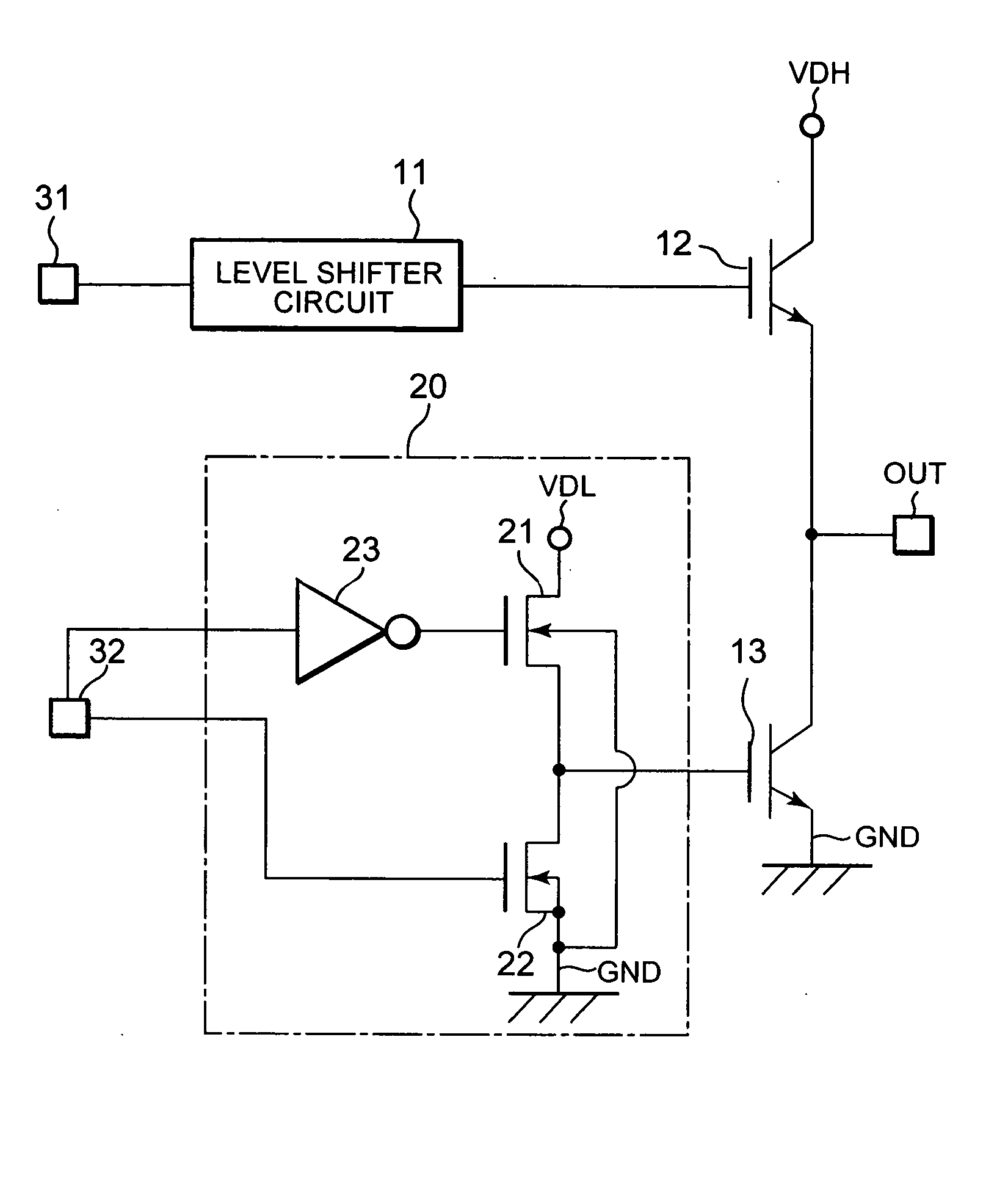
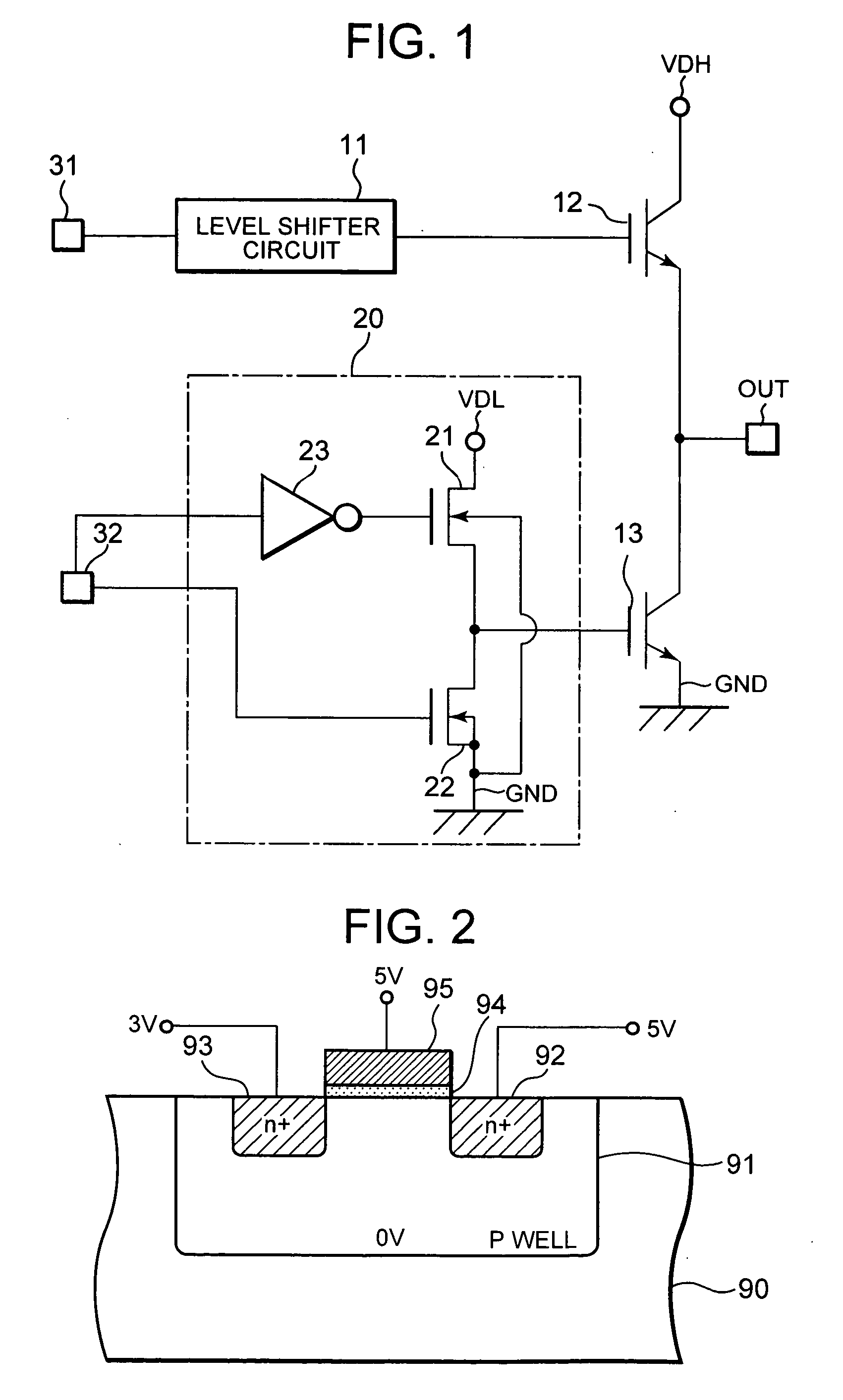
[0042]FIG. 1 is a circuit diagram of display apparatus driving circuitry of the invention. The display apparatus driving circuitry has a level shifter circuit 11, a buffer circuit 20, and two IGBTs 12 and 13.

[0043] The level shifter circuit 11 is constituted from a high-voltage-resistant PMOS or NMOS, not shown. Moreover, an input terminal 31 into which a signal (0 to 5 volts) is inputted from a control circuit, not shown, is connected to the level shifter circuit 11. The level shifter circuit 11 converts this signal into a signal of 0 to 100 volts, and inputs the converted signal into the gate of the IGBT 12.

[0044] The buffer circuit 20 is connected to an input terminal 32 into which a signal (0 to 5 volts) is inputted from a control circuit, not shown, and the output from the buffer circuit 20 is supplied to the gate of the IGBT 13.

[0045] The buffer circuit 20 in the display apparatus driving circuitry of the first embodiment is constituted from two NMOSs 21 and 22, and an inver...

fourth embodiment

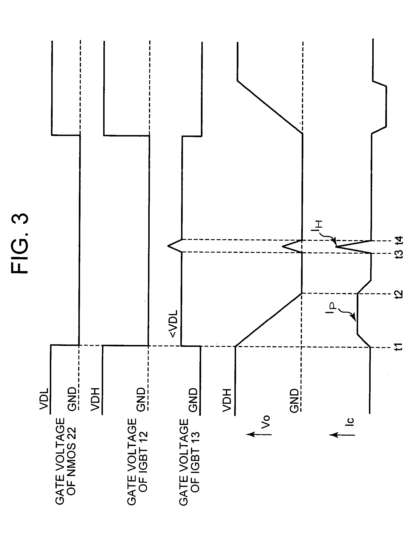
[0070] As described above, with the display apparatus driving circuitry according to the first to third embodiments of the invention, when the IGBT 13 is on its the gate potential is reduced below VDL by using a back gate effect. However, a second low-voltage power supply terminal VDL2 that supplies a voltage lower than VDL may instead be provided, whereby the gate potential, when on, can be reduced with a prescribed timing. This case will now be described as the invention.

[0071]FIG. 6 is a circuit diagram of the display apparatus driving circuitry of the fourth embodiment of the invention. With the display apparatus driving circuitry of the fourth embodiment shown here, only the buffer circuit is differs from the first embodiment. Therefore, for other constituent elements, the same reference numerals as in the first embodiment will be used, and description here will be omitted.

[0072] Unlike in the first to third embodiments, with the buffer circuit 60 of the fourth embodiment, pow...


PUM


Abstract

A display apparatus driving circuitry for driving a plasma display panel. A first transistor is electrically connected between an output terminal and a high-voltage power supply terminal. A second transistor is connected between the output terminal and a reference power supply terminal. A buffer circuit supplies a voltage lower than a low voltage VDL for logic to a gate of the second transistor to make a drop in an output waveform gradual during an address electrical discharge. In a preferred embodiment, during this drop in the output waveform, a p-channel type MOSFET of the buffer circuit is turned on, whereby the VDL is suppressed due to a back gate effect. Therefore, a signal at a potential lower than the VDL is inputted to the gate of the second transistor. As a result, the drop in the second transistor output waveform is gradual, so that noise and damage are prevented.

Description

BACKGROUND OF THE INVENTION [0001] 1. Field of the Invention [0002] The invention relates to display apparatus driving circuitry, and in particular relates to display apparatus driving circuitry for driving a plasma display panel. [0003] 2. Prior Art [0004] In recent years, plasma display panels (hereinafter referred to as ‘PDPs’), which can be made large in size and can be made thin and light-weight, have come into the limelight as display apparatuses in television broadcast receivers, personal computers and so on. FIG. 9 shows schematically an example of the constitution of a PDP driving apparatus for driving a PDP. [0005] For the sake of simplicity, the case of a two-electrode PDP 100 is shown in FIG. 9. The driving apparatus for the PDP 100 is constituted from a plurality of scan driver ICs (Integrated Circuits) 101-1, 101-2, 101-3, . . . , 101-n and data (address) driver ICs 102-1, 102-2, 102-3, . . . , 102-m and so on (here, n and m are arbitrary integers). [0006] The scan dri...

Claims


Application Information

Patent Timeline
Patent Type & Authority Applications(United States)
IPC IPC(8): G09G3/28G09G5/00
CPCG09G3/296G09G3/2932
Inventor KOBAYASHI, HIDETO
Owner FUJI ELECTRIC CO LTD
Why Eureka
Try Eureka