Scan testing mode control of gated clock signals for flip-flops

Inactive Publication Date: 2005-02-17
AVAGO TECH WIRELESS IP SINGAPORE PTE
View PDF12 Cites 4 Cited by
  • Summary
  • Abstract
  • Description
  • Claims
  • Application Information

AI Technical Summary

Benefits of technology

[0011] There are several benefits associated with the invention. First, the invention can be used to ensure that flip-flops receive a clock pulse in a controlled manner during testing, thereby facilitating more predictable test results. Second, the invention does not induce timing delays that would hinder normal operation of an integrated circuit.

Problems solved by technology

Scan testing does not test integrated circuit-level functionality.
The sheer number of flip-flops within an integrated circuit, which is often greater than a million, presents a daunting challenge for testing.
One challenge to providing effective scan testing is ensuring that the state of flip-flops only change during scan testing in a controlled manner.
When the state of flip-flops are not controlled during testing, they can impact other flip-flops in unpredictable ways leading to output patterns that do not correspond to reference patterns.
Furthermore, as processor speeds have increased, regulating clock inputs to flip-flops during scan testing has become more complicated.
Even slight delays on the order of picoseconds can potentially lead to erratic behavior in an integrated circuit.

Method used


Image

  • Scan testing mode control of gated clock signals for flip-flops
  • Scan testing mode control of gated clock signals for flip-flops
  • Scan testing mode control of gated clock signals for flip-flops

Examples


Embodiment Construction

[0018] While the present invention is described herein with reference to illustrative embodiments for particular applications, it should be understood that the invention is not limited thereto. Those skilled in the art with access to the teachings provided herein will recognize additional modifications, applications, and embodiments within the scope thereof and additional fields in which the invention would be of significant utility.

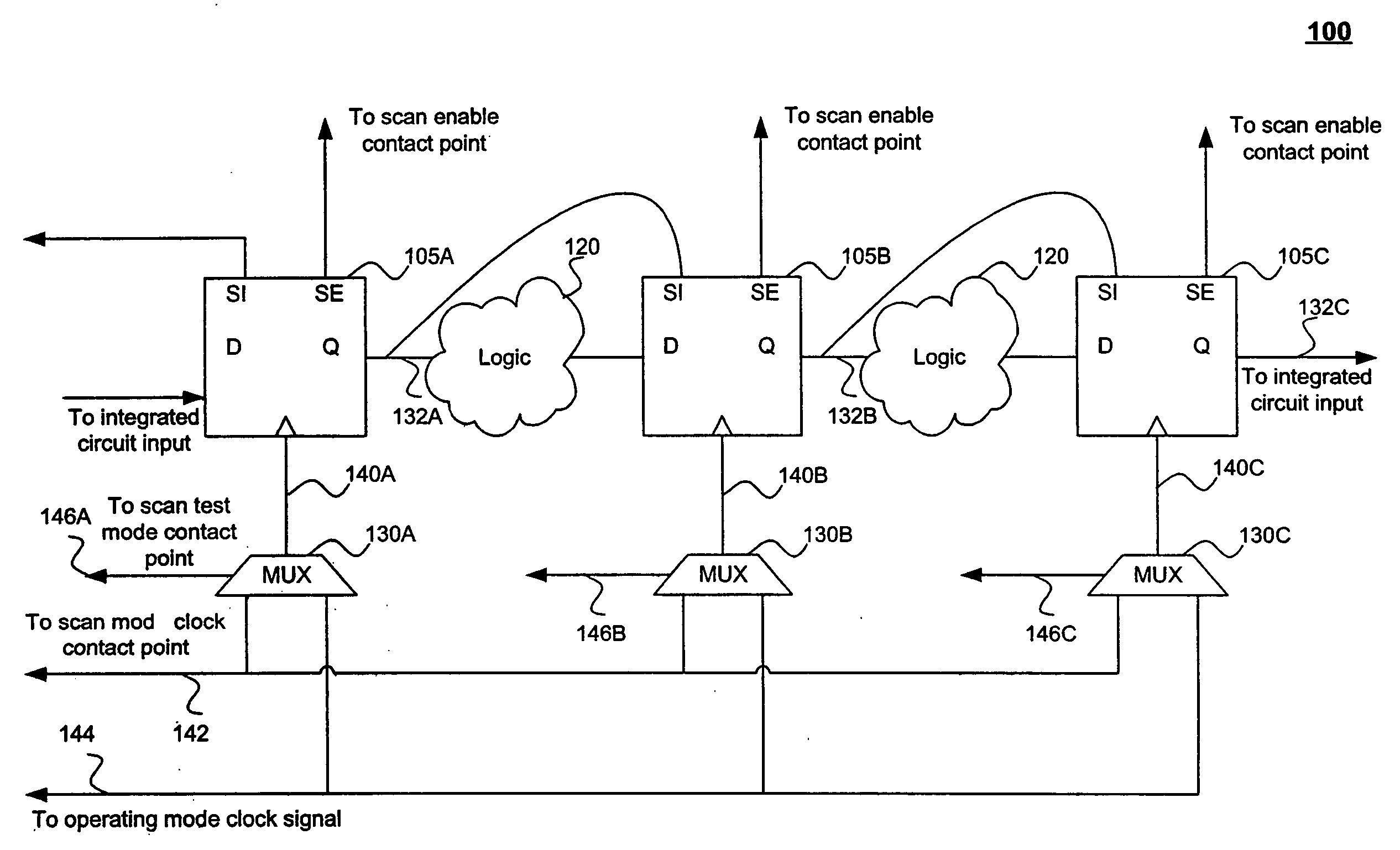
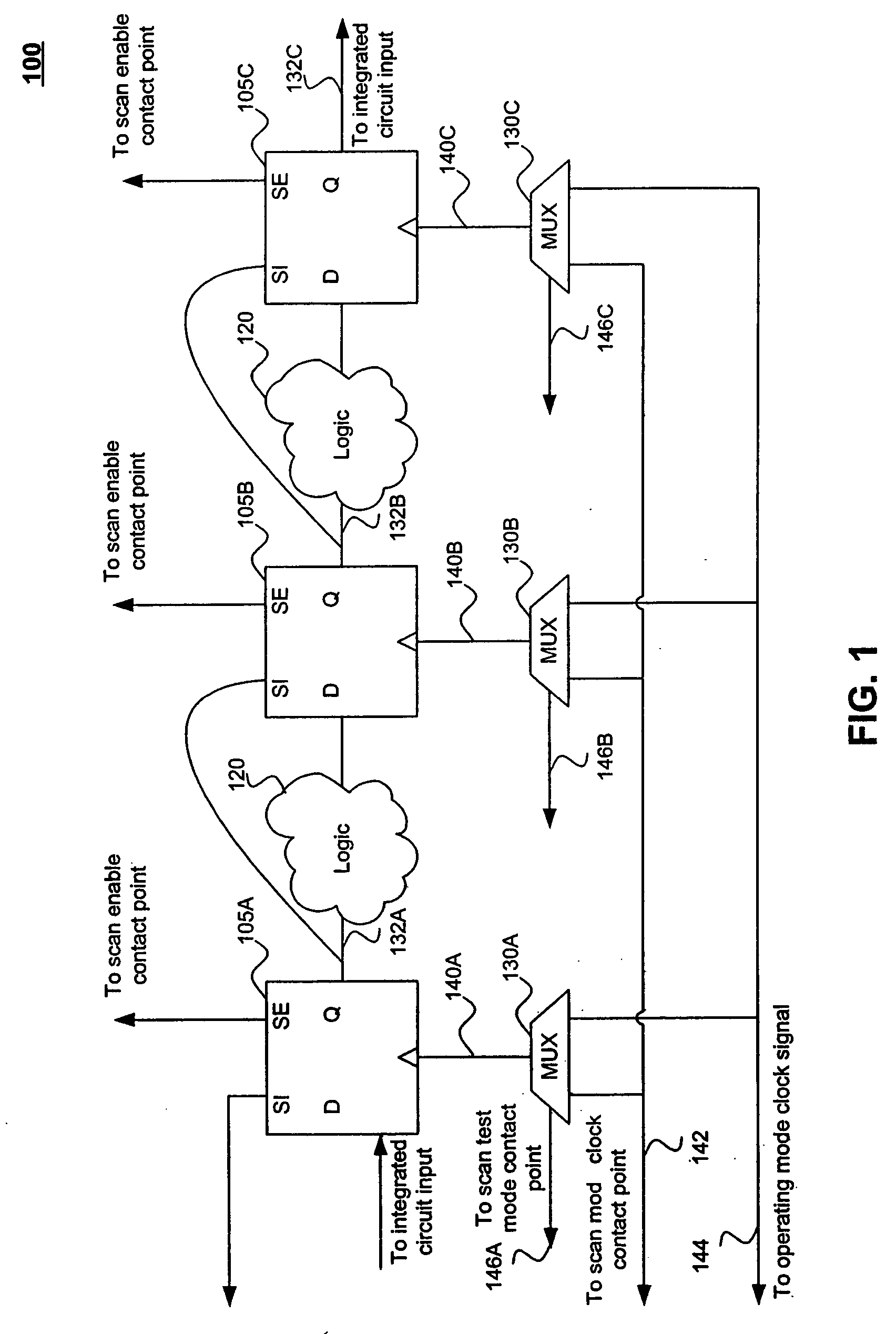
[0019]FIG. 1 illustrates an example of a truncated scan path within an integrated circuit. The scan path includes flip-flop 105A, flip-flop 105B, and flip-flop 105C. Flip-flop 105A represents the first flip-flop in the scan path. An SI input on flip-flop 105A is coupled to a scan input contact point. The scan input contact point provides an interface to an automated testing unit that allows test patterns to be inputted. An SE input on flip-flop 105A is coupled to a scan enable contact point.

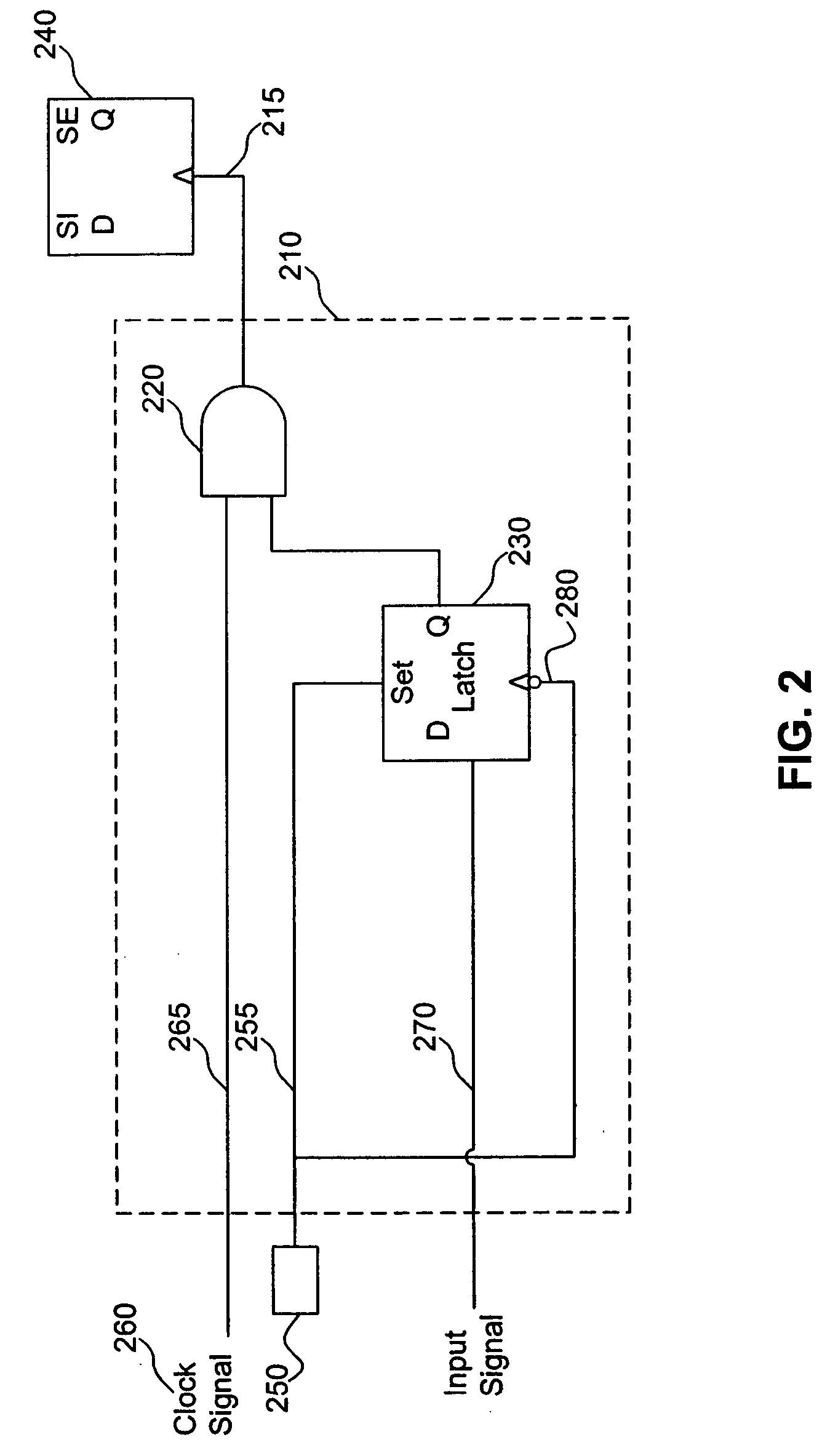
[0020] Two modes exist within scan testing: shift mode and cap...


PUM


Abstract

Circuits and a method to enhance scan testing by controlling clock pulses that are provided to flip-flops within an integrated circuit are provided. An integrated circuit is provided that includes a scan testing clock control circuit for flip-flops. The scan testing clock control circuit enables control of a clock input signal to one or more flip-flops within the integrated circuit. In one embodiment, a scan testing clock control circuit can be used to ensure that a flip-flop receives a clock input signal during scan testing. In one embodiment the scan testing clock control circuit includes a latch, and an AND gate. A method for scan testing using a scan testing clock control circuit for flip-flops is also provided.

Description

BACKGROUND OF THE INVENTION [0001] 1. Field of the Invention [0002] The present invention relates to integrated circuits, and more particularly, to scan testing of integrated circuits. [0003] 2. Background of Invention [0004] Effective testing of integrated circuits significantly enhances the ability of integrated circuit developers and manufacturers to provide reliable devices. Various techniques have been employed to test integrated circuits during the manufacturing process. One such technique that is commonly known, and has been used within the industry for over twenty years is scan testing. [0005] Scan testing provides an efficient approach to testing the structural integrity of devices, such as flip-flops, within a complex integrated circuit. Scan testing does not test integrated circuit-level functionality. Rather, test personnel use scan testing to confirm that individual flip-flops within an integrated circuit function properly. The sheer number of flip-flops within an integ...

Claims


Application Information

Patent Timeline
IPC IPC(8): H04N5/44H04N5/46H04N5/913
CPCH04N5/4401H04N5/46H04N2005/91364H04N21/426H04N21/4263H04N7/035
Inventor GUETTAF, AMAR
Owner AVAGO TECH WIRELESS IP SINGAPORE PTE
Why Eureka
Try Eureka