
Semiconductor device having electrical contact from opposite sides

a semiconductor and side-opposite technology, applied in the direction of semiconductor/solid-state device details, diodes, capacitors, etc., can solve the problems of non-ideal gate capacitor current leakage, limited utilization of such capacitors, waste of power consumption,

Inactive Publication Date: 2005-02-24
NORTH STAR INNOVATIONS
View PDF9 Cites 44 Cited by
  • Summary
  • Abstract
  • Description
  • Claims
  • Application Information

AI Technical Summary

Problems solved by technology

However, the advances in technologies are requiring the use of thin gate oxides that result in a non-ideal gate capacitor current leakage.
In addition, these capacitors consume valuable circuit layout area and thus the utilization of such capacitors is limited.
Gate capacitor current leakage also results in wasted power consumption that is critical in low-power applications.
Because of a large distance between the decoupling capacitor and active circuitry, the high frequency response of the decoupling capacitor is limited.
The distance must be large because placement of the decoupling capacitor is limited and typical placement of the decoupling capacitor is further removed from active circuitry than desired.
Existing decoupling capacitor structures therefore either suffer from power consumption issues, size issues and / or electrical efficiency.

Method used


Image

  • Semiconductor device having electrical contact from opposite sides
  • Semiconductor device having electrical contact from opposite sides
  • Semiconductor device having electrical contact from opposite sides

Examples


Embodiment Construction

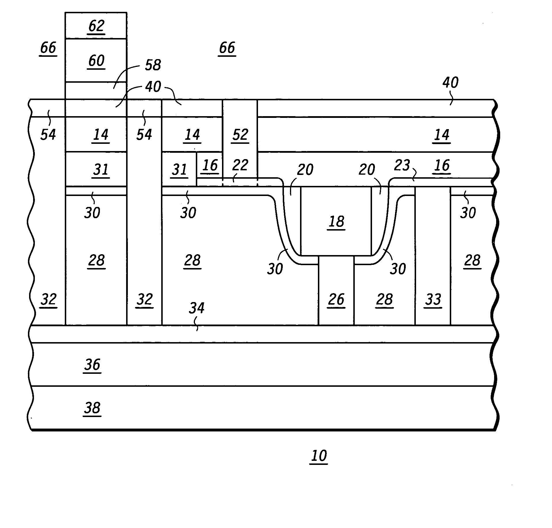
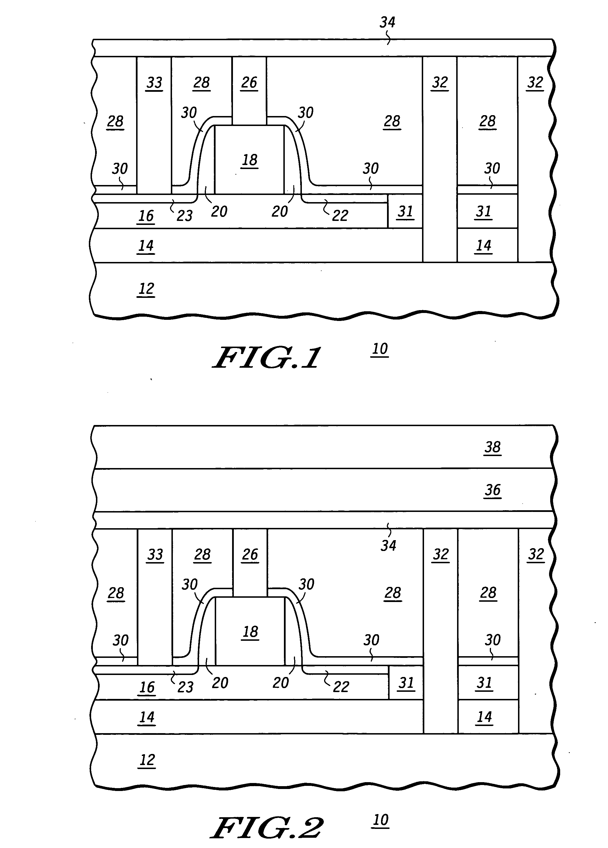
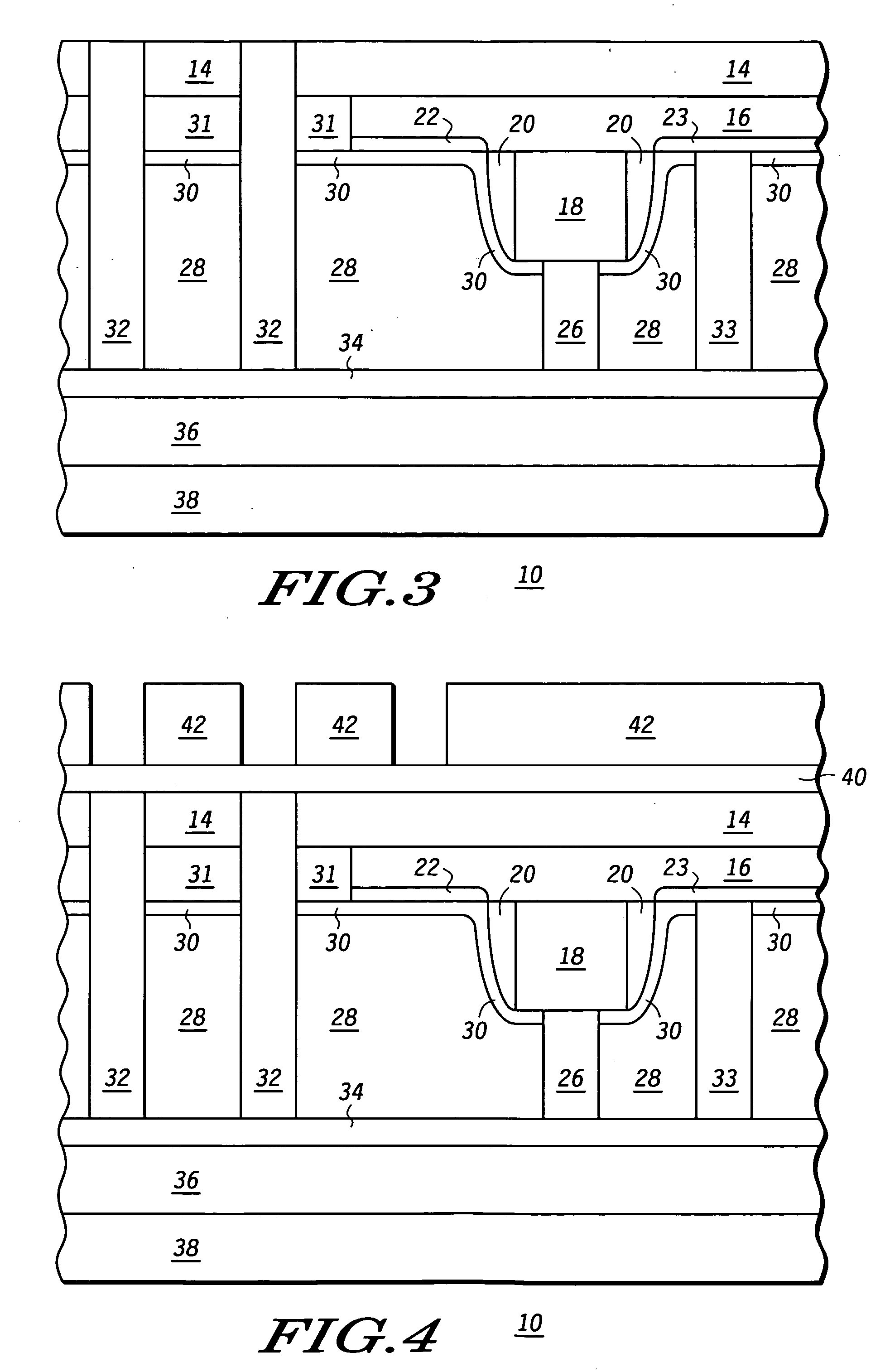
[0007] Illustrated in FIG. 1 is a semiconductor device 10 in accordance with the present invention. It should be understood that the terms “over”, “overlying” and “above” are defined herein for layers and structures formed with respect to the specific orientation of each figure discussed herein. For example, in FIGS. 1, 2 and 19, the term “over” is used with reference to anything vertically above the illustrated substrate 12. However, the illustrations of FIGS. 3-18 provide an inverse orientation of FIGS. 1, 2 and 19. The term “over” will continue to be used in the discussion even though such structures are actually below substrate 12 with respect to the original orientation of FIGS. 1 and 2. It should also be apparent that semiconductor device 10 and all embodiments thereof is operational not only in the illustrated orientations but also at any orientation, whether 90, 180 degrees or any other orientation. Also, multiple implementations of semiconductor device 10 may be made wherei...


PUM


Abstract

A semiconductor (10) has an active device, such as a transistor, with a directly underlying passive device, such as a capacitor (75, 77, 79), that are connected by a via or conductive region (52) and interconnect (68, 99). The via or conductive region (52) contacts a bottom surface of a diffusion or source region (22) of the transistor and contacts a first (75) of the capacitor electrodes. A laterally positioned vertical via (32, 54, 68) and interconnect (99) contacts a second (79) of the capacitor electrodes. A metal interconnect or conductive material (68) may be used as a power plane that saves circuit area by implementing the power plane underneath the transistor rather than adjacent the transistor.

Description

FIELD OF THE INVENTION [0001] This invention relates generally to integrated circuits, and more specifically, to making electrical contact to semiconductor circuit elements. BACKGROUND OF THE INVENTION [0002] Present day semiconductors utilize decoupling capacitors built using transistor gates. Decoupling capacitors are needed to prevent voltage drops in the internal supplies of an integrated circuit when large amounts of switching activity occur. However, the advances in technologies are requiring the use of thin gate oxides that result in a non-ideal gate capacitor current leakage. In addition, these capacitors consume valuable circuit layout area and thus the utilization of such capacitors is limited. Gate capacitor current leakage also results in wasted power consumption that is critical in low-power applications. The leakage may be mitigated, but at the expense of total decoupling capacitance and process complexity. Because of a large distance between the decoupling capacitor a...

Claims


Application Information

Patent Timeline
Patent Type & Authority Applications(United States)
IPC IPC(8): H01L21/02H01L21/768H01L21/84H01L23/48H01L23/522H01L27/06H01L27/12
CPCH01L21/76838H01L21/76898H01L21/84H01L23/481H01L23/5223H01L27/0688H01L2924/0002H01L27/1203H01L28/40H01L2924/00H01L27/0629
Inventor SANCHEZ, HECTORMENDICINO, MICHAEL A.MIN, BYOUNG W.YU, KATHLEEN C.
Owner NORTH STAR INNOVATIONS
Learn More