Thin film capacitor and method of manufacturing the same

a technology capacitors, applied in the field of thin film capacitors, can solve the problems of difficult to provide highly reliable thin film capacitors

Inactive Publication Date: 2005-03-17
FUJITSU LTD
View PDF8 Cites 17 Cited by
  • Summary
  • Abstract
  • Description
  • Claims
  • Application Information

AI Technical Summary

Benefits of technology

[0011] The thin film capacitor of the invention comprises an insulating substrate, a capacitor structure located on the substrate, the capacitor structure having a dielectric layer sandwiched between a lower electrode layer and an upper electrode layer, and conductor members respectively connected to the lower electrode layer and the upper electrode layer, the thin film capacitor being characterized in that at least the dielectric layer has a side face having a sufficient slope for preventing the short circuit of the upper electrode layer with the lower electrode layer through the conductor member.
[0014] (b) in the case where there is no conductor member penetrating the lower electrode layer, forming the upper electrode layer and the dielectric layer by patterning the films for the upper electrode layer and the dielectric layer together by an ion milling process, and performing the patterning by an ion milling process so as to afford a slope to the side face of at least the dielectric layer, the slope being sufficient for preventing a short circuit of the upper electrode layer with the lower electrode layer through the conductor member.

Problems solved by technology

However, in this case, rerouting the wiring line between the chip capacitor and the LSI chip on the circuit board is necessary and there is an inductance between leads for the rerouting.
Accordingly, with this method it is difficult to provide highly reliable thin film capacitors.

Method used


Image

  • Thin film capacitor and method of manufacturing the same
  • Thin film capacitor and method of manufacturing the same
  • Thin film capacitor and method of manufacturing the same

Examples


example 1

[0035] Via holes of 60 micrometers in diameter were formed in a glass substrate at a 150 micrometers pitch by a dry etching process using CF4 gas. An insulating film of SiO2 was deposited on the inner walls of the resultant via holes by a CVD process, after which a conductor (Pt) was filled in the via holes to prepare a substrate with through holes.

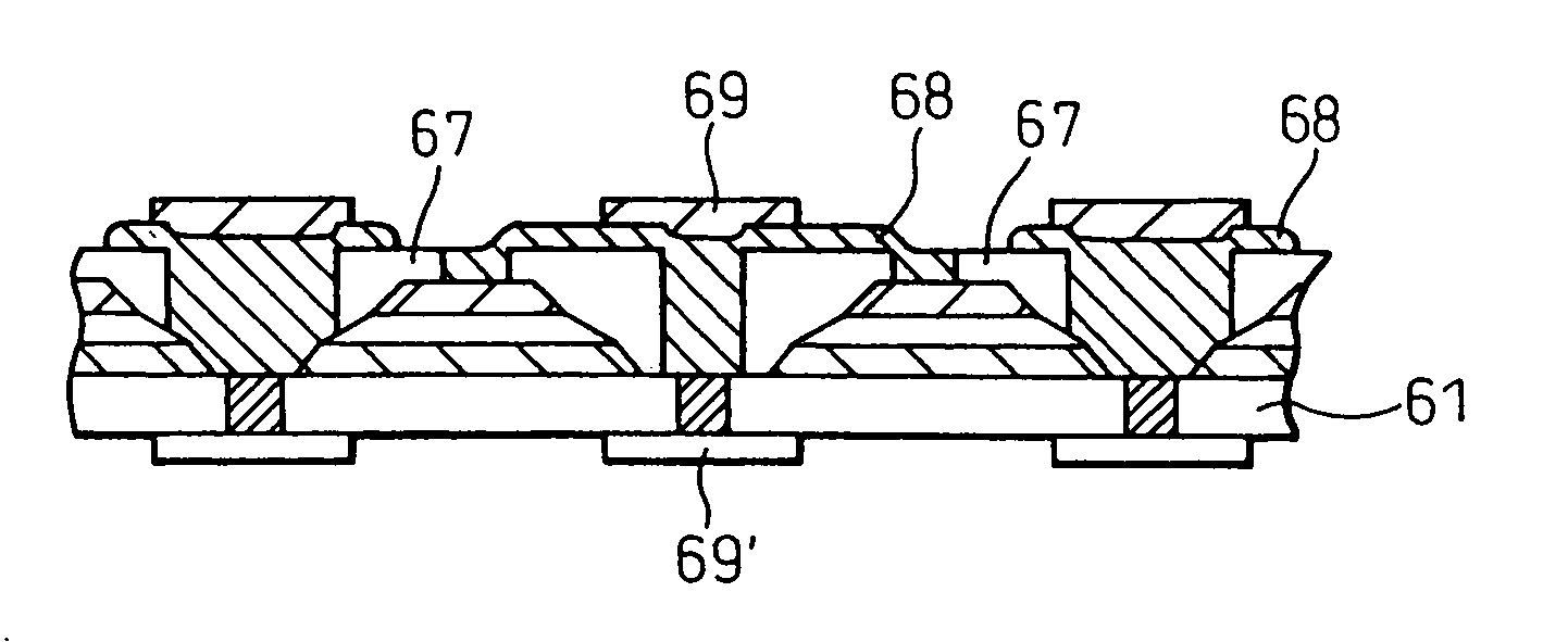
[0036] As shown in FIG. 5A, on the glass substrate 61 thus prepared having the conductor 62 filled in the via holes therein, successive films of TiO2 (0.05 micrometer) and Pt (0.2 micrometer), as materials for a lower electrode were formed by a sputtering process, to provide a film 63 for the lower electrode layer. The TiO2 sputtering was carried out at room temperature, being followed by annealing at 650° C. At the subsequent Pt sputtering, the substrate was at a temperature of 550° C. In the same vacuum system, a film of (Ba, Sr)TiO3 (hereinafter called BST) of a high dielectric constant material was then formed by sputtering, to provi...

example 2

[0039] Thin film capacitors were fabricated in the same manner as in Example 1, except that the formation of BST dielectric film 64 (FIG. 5A) was done using a sol-gel process.

[0040] The formation of BST dielectric film was carried out as follows. A preliminarily fired film having a certain thickness was obtained by repeating two times a series of procedures in which a coated film of about 100 nanometers thick was prepared from a starting solution for BST containing three alkoxides each having one of metal elements Ba, Sr and Ti by a spin coat process (2000 rpm, 30 seconds), and was dried at 120° C. and provisionally fired at 400° C. The preliminarily fired film was then finally fired in earnest at 650° C., to thereby crystallize the BST to provide the film 64 for a dielectric layer.

example 3

[0041] A substrate with through holes was prepared by forming via holes having a diameter of 50 micrometers in a 0.2 millimeter thick sapphire substrate at a 200 micrometers pitch by a laser beam, and filling a conductor (Pt) in the via holes by an MOCVD process. Using this substrate, thin film capacitors were fabricated as in Example 1.

[0042] As described, according to the invention, there can be provided a thin film capacitor having improved reliability because it can be manufactured by simultaneously patterning all films constructing the capacitor (films for electrode layers and a film for a dielectric layer), and not separately patterning the layers with each formation of one of the films for electrode and dielectric layers, which can be the cause of inclusion of impurities and particles in the films. In addition, the simultaneous patterning of the films makes the successive formation of the films possible and, accordingly, can contribute to the improvement of a production effi...


PUM


Abstract

A thin film capacitor comprising an insulating substrate, a capacitor structure located on the substrate, the capacitor structure having a dielectric layer sandwiched between a lower electrode layer and an upper electrode layer, and conductor members respectively connected to the lower electrode layer and the upper electrode layer, wherein at least the dielectric layer has a side face having a sufficient slope for preventing the short circuit of the upper electrode layer with the lower electrode layer through the conductor member. A method of manufacturing such a thin film capacitor is also disclosed.

Description

CROSS-REFERENCE TO RELATED APPLICATIONS [0001] This application is based upon and claims the benefit of priority from prior Japanese Patent Application No. 2001-394512, filed on Dec. 26, 2001, the entire contents thereof being incorporated herein by reference. BACKGROUND OF THE INVENTION [0002] 1. Field of the Invention [0003] The invention relates to a thin film capacitor, and particularly to a thin film capacitor capable of stably operating in a high frequency region (GHz band) when used in a digital LSI operating at a high speed. [0004] 2. Description of the Related Art [0005] Recent digital LSIS (large-scale integrated circuits), including microprocessors, are designed to have a high speed and a low power consumption. Accordingly, decoupling capacitors (also called bypass capacitors) are required to have an improved performance, the decoupling capacitor suppressing a change in the power supply voltage when an impedance load on an LSI is abruptly changed, to thereby decrease swit...

Claims


Application Information

Patent Timeline
Patent Type & Authority Applications(United States)
IPC IPC(8): H01L21/02H01G4/33H01L21/768H01L23/50H01L27/01H01L27/108H01L27/13
CPCH01L21/76804H01L21/76895H01L23/50H01L27/016H01L27/13H01L28/40H01L2924/0002H01L28/55H01L2924/3011H01L2924/00
Inventor SHIOGA, TAKESHIBANIECKI, JOHN DAVIDKURIHARA, KAZUAKI
Owner FUJITSU LTD
Why Eureka
Try Eureka