Content addressable memory with configurable class-based storage partition

a content addressable and class-based technology, applied in the field of semiconductor memories, can solve problems such as unsatisfactory power drawing

Inactive Publication Date: 2005-03-24
AVAGO TECH INT SALES PTE LTD
View PDF71 Cites 16 Cited by
  • Summary
  • Abstract
  • Description
  • Claims
  • Application Information

AI Technical Summary

Problems solved by technology

This can cause an undesirable amount of power to be drawn during the compare operation.

Method used


Image

  • Content addressable memory with configurable class-based storage partition
  • Content addressable memory with configurable class-based storage partition
  • Content addressable memory with configurable class-based storage partition

Examples


Embodiment Construction

In the following description, for purposes of explanation, specific nomenclature is set forth to provide a thorough understanding of the present invention. However, it will be apparent to one skilled in the art that these specific details may not be required to practice the present invention. In other instances, well-known circuits and devices are shown in block diagram form to avoid obscuring the present invention unnecessarily. Additionally, the interconnection between circuit elements or blocks may be shown as buses or as single signal lines. Each of the buses may alternatively be a single signal line, and each of the single signal lines may alternatively be buses. In addition, the logic levels assigned to various signals in the description below are arbitrary, and therefore may be modified (e.g., reversed polarity) as desired.

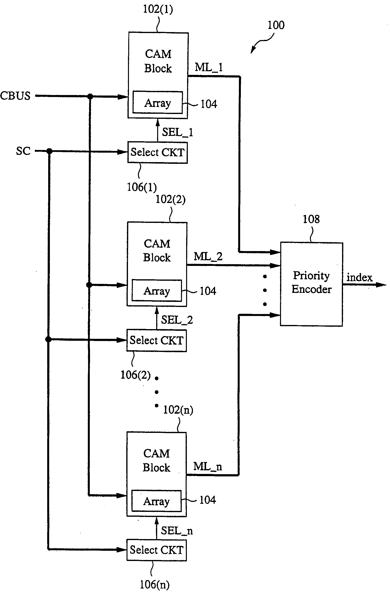
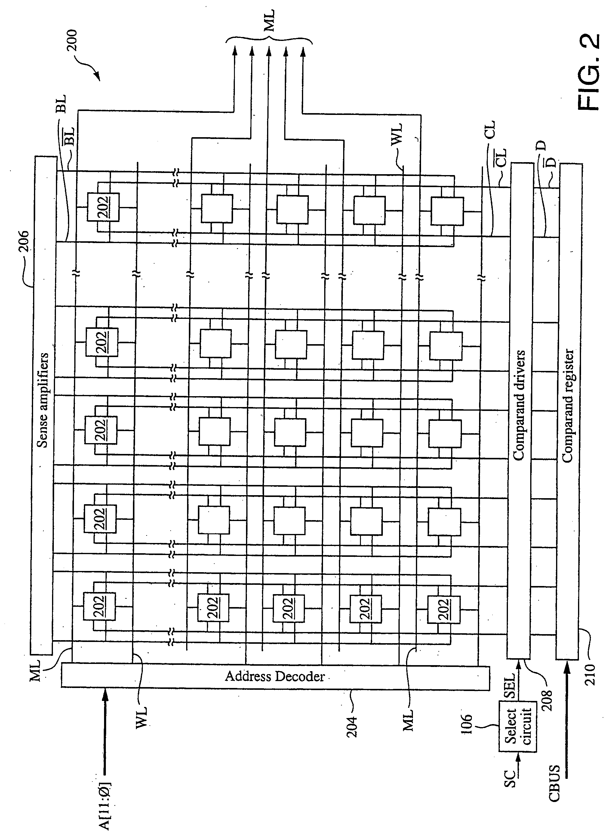
Embodiments of the present invention are discussed below in the context of a CAM device 100 for simplicity only. It is to be understood that embodiments...


PUM


Abstract

A content addressable memory (CAM) device having a plurality of CAM blocks and a block selection circuit. Each of the CAM blocks includes an array of CAM cells to store data words having a width determined according to a configuration value. The block selection circuit includes an input to receive a class code and circuitry to output a plurality of select signals to the plurality of CAM blocks. Each of the select signals selectively disables a respective one of the plurality of CAM blocks from participating in a compare operation according to whether the class code matches a class assignment of the CAM block.

Description

FIELD OF INVENTION This invention relates generally to semiconductor memories and more particularly to content addressable memories. BACKGROUND Content addressable memories (CAMs) are frequently used for address look-up functions in Internet data routing. For example, routers used by local Internet Service Providers (ISPs) typically include one or more CAMs for storing a plurality of Internet addresses and associated data such as, for instance, corresponding address routing information. When data is routed to a destination address, the destination address is compared with all CAM words, e.g., Internet addresses, stored in the CAM array. If there is a match, routing information corresponding to the matching CAM word is output and thereafter used to route the data. A CAM device includes a CAM array having a plurality of memory cells arranged in an array of rows and columns. Each memory cell stores a single bit of digital information, i.e., either logic zero or logic one. The bits s...

Claims


Application Information

Patent Timeline
Patent Type & Authority Applications(United States)
IPC IPC(8): G06F17/30G11C15/00G11C15/04
CPCG06F17/30982G11C15/04G11C15/00G06F16/90339
Inventor PEREIRA, JOSE P.SRINIVASAN, VARADARAJAN
Owner AVAGO TECH INT SALES PTE LTD
Why Eureka
Try Eureka