Semiconductor device

Inactive Publication Date: 2005-03-31
RENESAS ELECTRONICS CORP
View PDF3 Cites 7 Cited by
  • Summary
  • Abstract
  • Description
  • Claims
  • Application Information

AI Technical Summary

Benefits of technology

[0006] An object of the present invention is to provide a high breakdown voltage diode suitable for integration.
[0007] In an aspect of the present invention, a semiconductor device includes a plurality of first diffusion regions of a first conductive type formed on a diffusion layer well of the first conductive type; and a plurality of second diffusion regions of a second conductive type form

Problems solved by technology

However, in the structure of the above-mentioned conventional high breakdown voltage diode, in order to need a large region for improvement of the breakdown voltage, the high integration becomes difficult.

Method used


Image

  • Semiconductor device
  • Semiconductor device
  • Semiconductor device

Examples


first embodiment

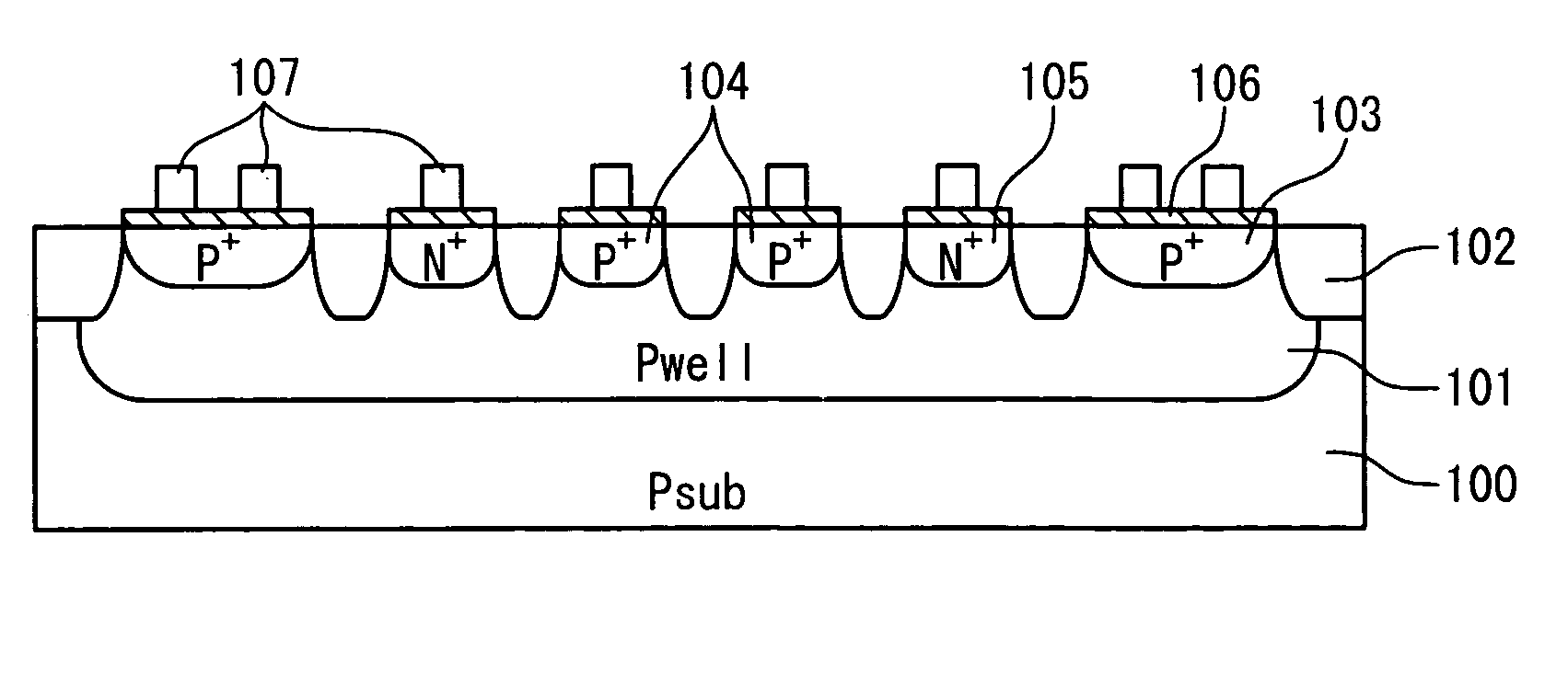
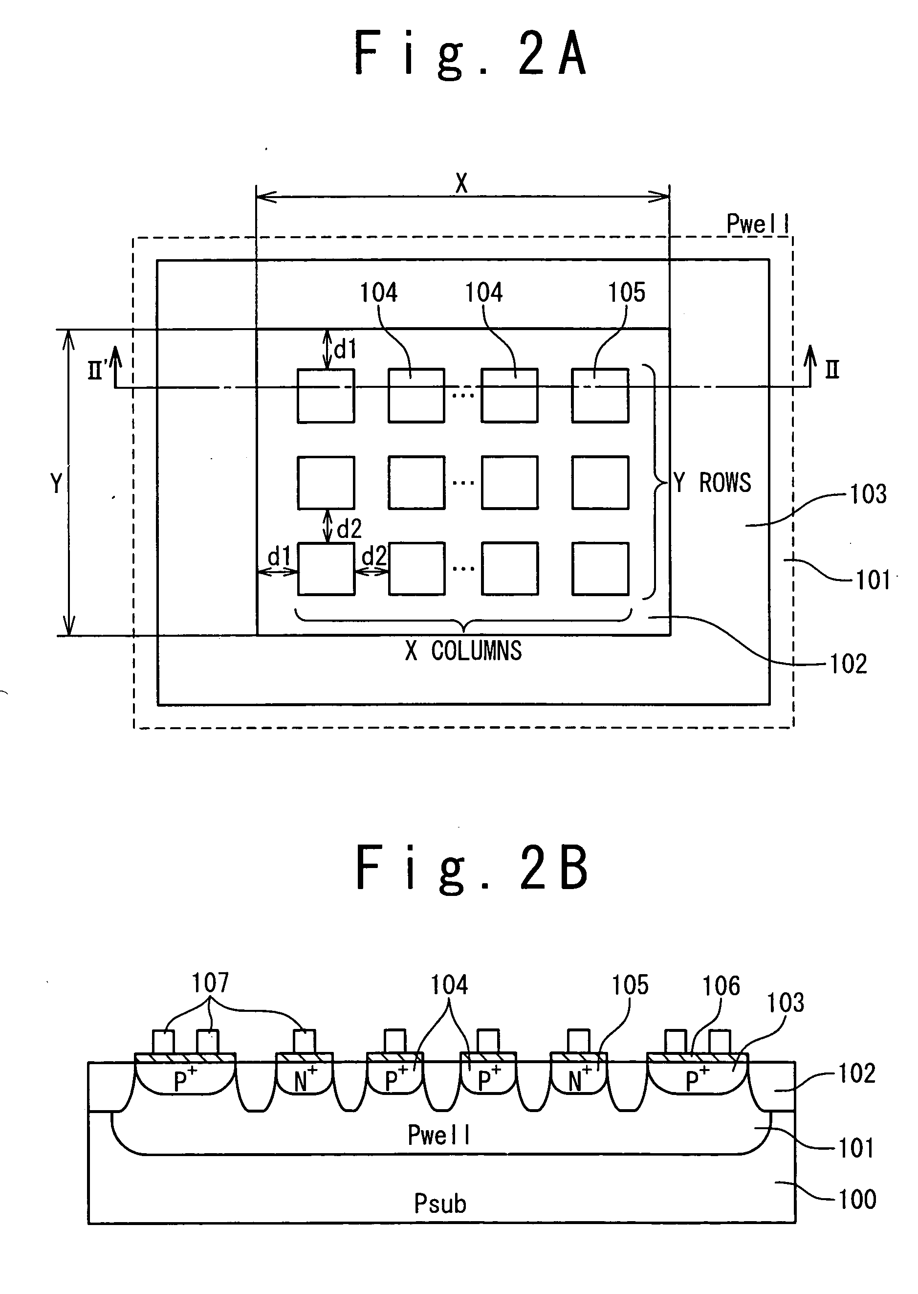
[0021] As shown in FIG. 2A, in the present invention, a P-type well 101 is formed in a P-type semiconductor substrate 100 as a P-type embedded diffusion layer to have a higher impurity concentration than that of the P-type semiconductor substrate 100. A P+-type diffusion layer 103 is formed in the P-type well 101 in a ring along an outer circumference of the P-type well 101. A plurality of N+-type rectangular diffusion regions 105 and a plurality of P+-type rectangular diffusion regions 104 are provided in a region of the P-type well 101 surrounded by the P+-type diffusion layer 106. The P+-type diffusion region 104 has a higher impurity concentration higher than that of the P-type well 101. A device separation region (insulation region) 102 is formed in the outer circumference of the P-type well 101 to contact the P-type semiconductor substrate 100 and the P-type well 101. Other device separation region are formed between the diffusion regions to insulate them from each other but d...

third embodiment

[0030] Also, in the diode according to the present invention, the shape of each of P+-type diffusion region 604 and N+-type diffusion region 605 is triangular, as shown in FIG. 7. In this case, the circumference length can be made larger, compared with a case that each diffusion region is rectangular. Therefore, the EDS breakdown voltage can be further improved. The definitions of the distances d1 and d2 are same as in the above embodiments.

fourth embodiment

[0031] Moreover, in the diode according to the present invention, the shape of each of P+-type diffusion region and N+-type diffusion region is hexagonal, as shown in FIG. 8. In this case, the region surrounded by the P+-type diffusion layer 103 in the ring can be effectively utilized. In this case, the diffusion region arranged in the outermost portion of the surrounded region is desired to have a part of the hexagonal shape, as shown in FIG. 8. Also, the P+-type diffusion region and N+-type diffusion region may be arranged alternately in the vertical direction or in the horizontal and vertical directions. In either case, the circumference length is same.

[0032] As described above, according to the semiconductor device of the present invention, the opposing area can be made large between the different conductive type diffusion regions so that the endurance can be improved even in case of the same area, compared with the conventional structure.


PUM


Abstract

In a semiconductor device, a plurality of first diffusion regions of a first conductive type are formed on a diffusion layer well of the first conductive type. A plurality of second diffusion regions of a second conductive type are formed on the diffusion layer well of the first conductive type. An impurity concentration of each of the plurality of first and second diffusion regions is desirably higher than that of the diffusion layer well. The plurality of first diffusion regions are connected to a first common node as an anode and the plurality of second diffusion regions are connected to a second common node as a cathode.

Description

BACKGROUND OF THE INVENTION [0001] 1. Field of the Invention [0002] The present invention relates to a semiconductor device, more particularly to a protection element to protect an internal circuit of a semiconductor device. [0003] 2. Description of the Related Art [0004] In recent years, in order to protect the internal circuit of an IC from current of electrostatic serge, a protection element is provided for the input terminal. As this protection element, a diode with a high breakdown voltage is generally used. FIGS. 1A and 1B show such a conventional high breakdown voltage diode. Referring to FIGS. 1A and 1B, in the conventional diode, a P-type well 801 is formed in a P-type semiconductor substrate 800, and a P+-type diffusion layer 803 is formed in a ring along an outer circumference of the P-type well 801 to have a higher impurity concentration than the P-type well 801. An N+-type diffusion layer 804 is formed in a region of the P-type well 801 surrounded by the P+-type diffusi...

Claims


Application Information

Patent Timeline
IPC IPC(8): H01L21/822H01L21/761H01L23/60H01L23/62H01L27/04H01L29/06H01L29/861H01L29/866
CPCH01L29/866H01L29/0692
Inventor TANAKA, KOUJI
Owner RENESAS ELECTRONICS CORP
Why Eureka
Try Eureka