Method and apparatus for using cobalt silicided polycrystalline silicon for a one time programmable non-volatile semiconductor memory

a technology of cobalt silicided polycrystalline silicon and semiconductor memory, which is applied in the direction of electrical apparatus, semiconductor devices, semiconductor/solid-state device details, etc., can solve the problems of low junction breakdown voltage, rendering anti-fuse devices less compatible with these advanced circuits, and certain anti-fuse materials are not compatible with standard cmos fabrication processes

Active Publication Date: 2005-03-31
AVAGO TECH INT SALES PTE LTD
View PDF19 Cites 17 Cited by
  • Summary
  • Abstract
  • Description
  • Claims
  • Application Information

AI Technical Summary

Benefits of technology

[0014] The invention comprises a fusible link device disposed on a semiconductor substrate comprising a first material layer having a first sheet resistance and a second material layer having a second sheet resistance overlying the first material layer. The second sheet resistance is less than the first sheet resistance. The fusible link is programmable to an opened state in which an opening is formed in the first and the second material layers. In a closed state the first and the second material layers provide a current path therethrough.
[0015] The invention further comprises a method for forming a f

Problems solved by technology

But higher doping levels in advanced integrated circuit devices result in lower junction breakdown voltages, rendering anti-fuse devices less compatible with these advanced circuits.
Also, certain of the anti-fuse materials are not compatible with standard CMOS fabrication processes.
Disadvantageously, according to the prior art, the fo

Method used


Image

  • Method and apparatus for using cobalt silicided polycrystalline silicon for a one time programmable non-volatile semiconductor memory
  • Method and apparatus for using cobalt silicided polycrystalline silicon for a one time programmable non-volatile semiconductor memory
  • Method and apparatus for using cobalt silicided polycrystalline silicon for a one time programmable non-volatile semiconductor memory

Examples


Embodiment Construction

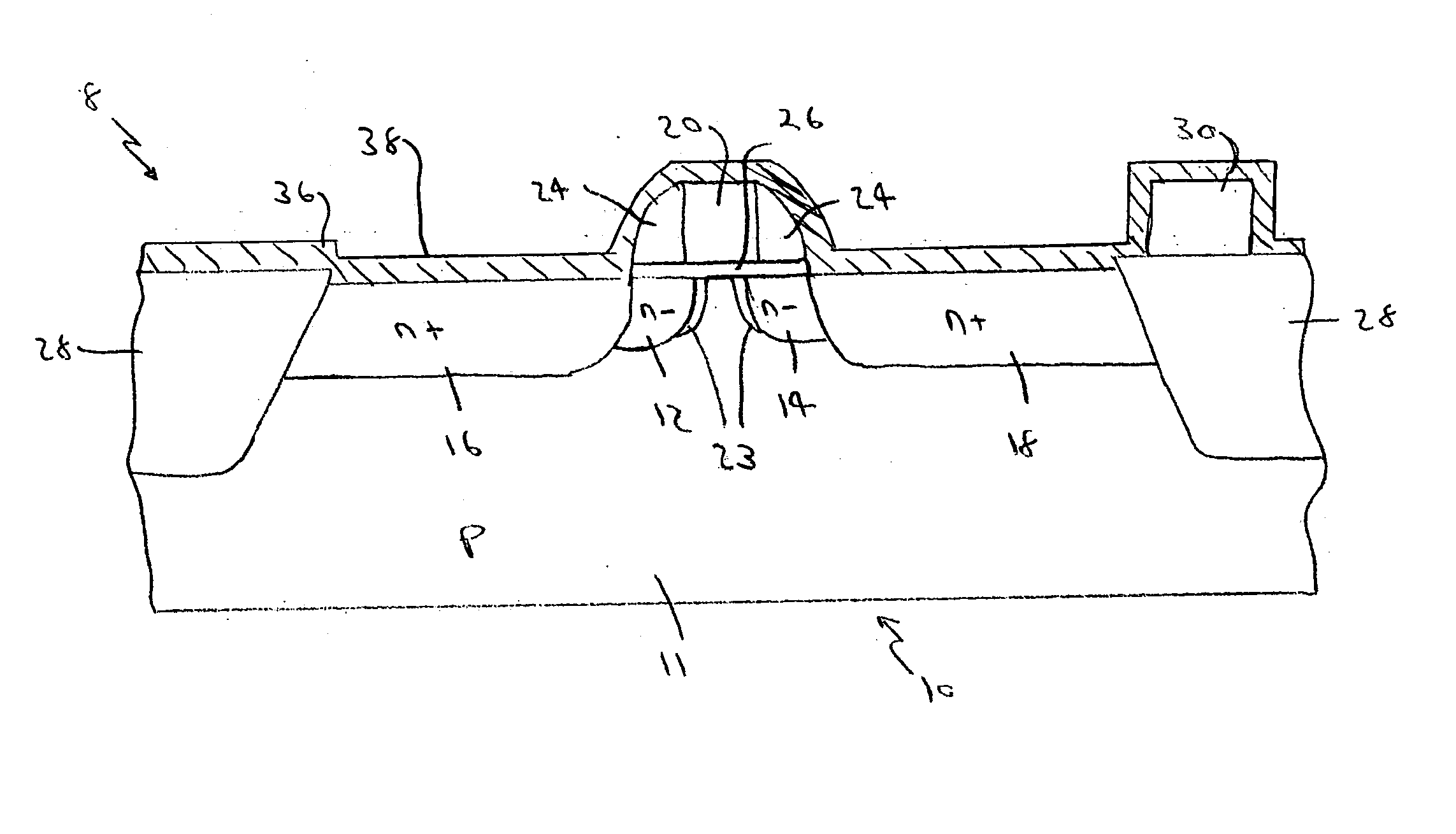
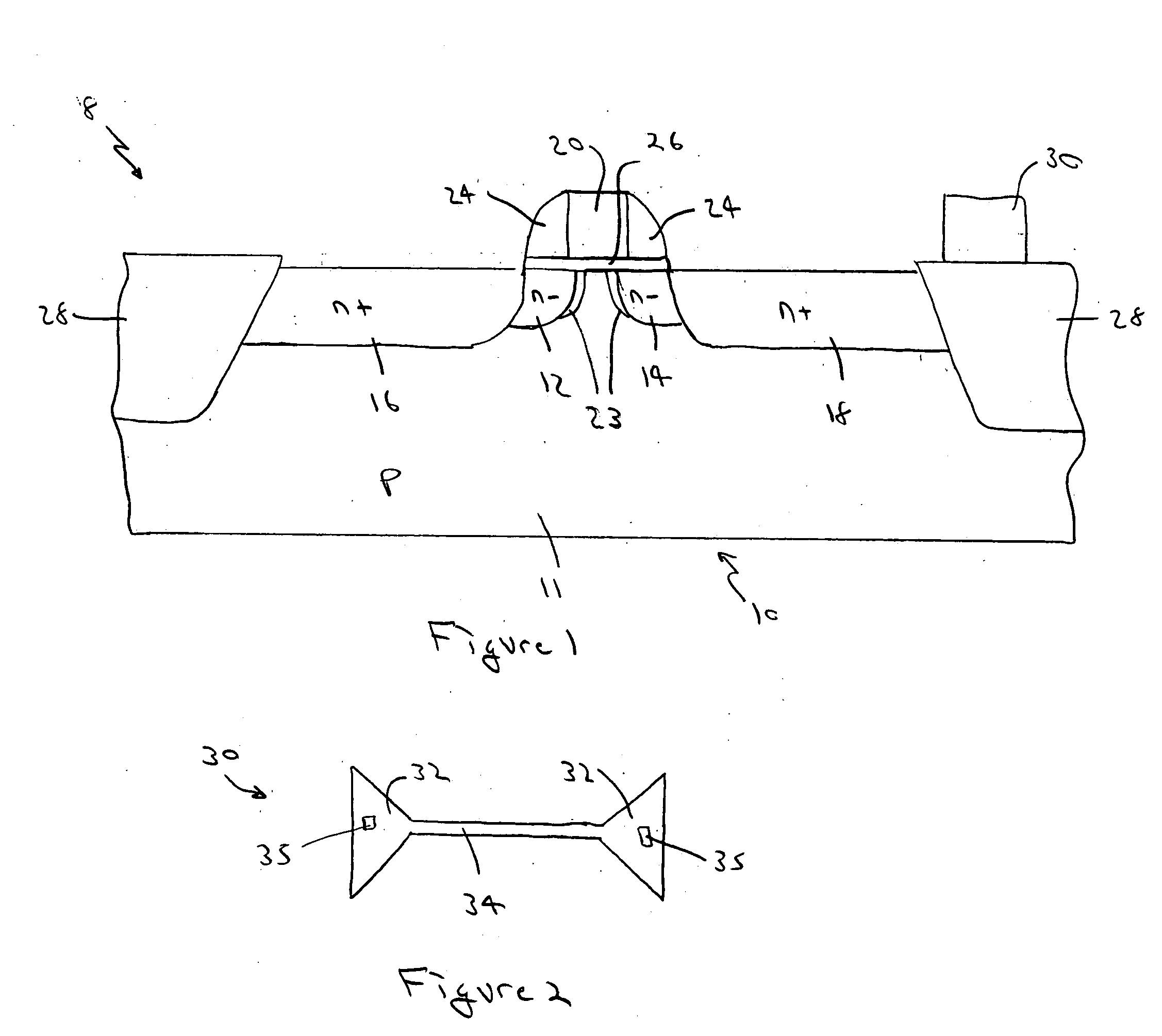
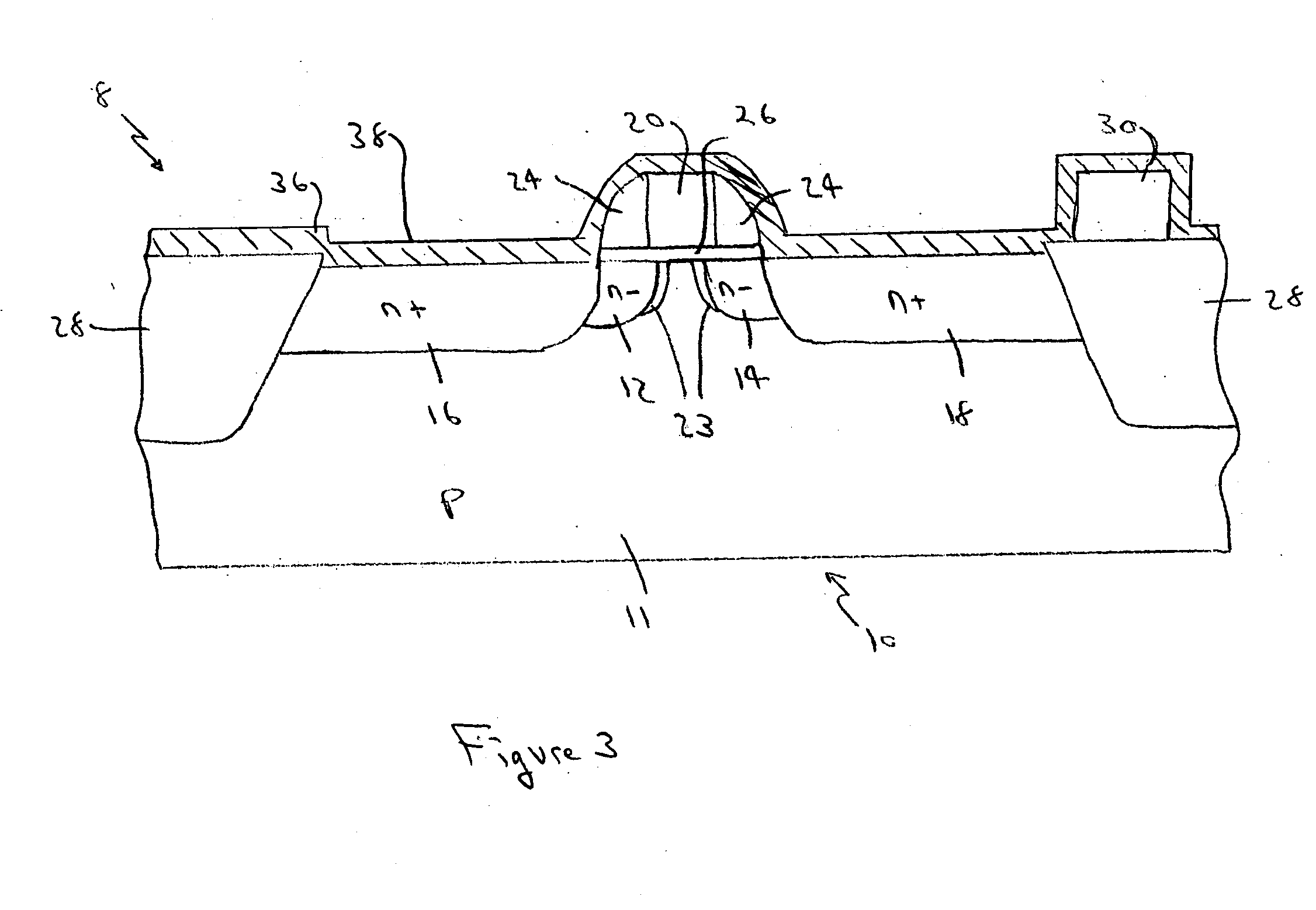
[0023] Before describing in detail the particular method and apparatus for forming a one-time programmable non-volatile memory element on a semiconductor chip, it should be observed that the present invention resides primarily in a novel and non-obvious combination of elements and process steps. Accordingly, the inventive elements and steps have been represented by conventional elements and steps in the drawings, showing only those specific details that are pertinent to the present invention so as not to obscure the disclosure with details that will be readily apparent to those skilled in the art having the benefit of the description herein.

[0024] After forming the doped regions in a semiconductor substrate, the regions must be connected to form operative devices that perform the desired circuit functions. These connections, referred to as conductive interconnects or metallization structures, are formed using known photolithographic and deposition techniques, and comprise substanti...


PUM


Abstract

A fusible link formed on a semiconductor substrate. The fusible link comprises a silicide layer overlying a polysilicon layer. The fusible link is programmed to an open state by passing a current therethrough that opens the polysilicon and the silicide layers.

Description

FIELD OF THE INVENTION [0001] This invention relates generally to semiconductor integrated circuit fabrication technologies and more specifically to a one-time programmable non-volatile memory. BACKGROUND OF THE INVENTION [0002] Memory devices for storing digital data are abundant in today's computers, automobiles, cellular telephones and media information cards. Certain of these memory devices or storage elements, referred to as non-volatile memory, retain the stored digital data when power is removed from the device. For example non-volatile memory instructions instruct a computer during the boot-up process and store instructions and data for sending and receiving calls in a cellular telephone. Electronic products of all types, from microwave ovens to heavy industrial machinery, store their operating instructions in non-volatile storage elements. Certain non-volatile memory devices offer multiple programming capabilities, with previously stored information overwritten by new data....

Claims


Application Information

Patent Timeline
IPC IPC(8): H01L21/336H01L23/525H01L29/78
CPCH01L23/5256H01L29/665H01L29/6659H01L2924/0002H01L29/7833H01L2924/00
Inventor HUI, FRANK YAUCHEE
Owner AVAGO TECH INT SALES PTE LTD
Why Eureka
Try Eureka