EL display device, driving method thereof, and electronic equipment provided with the display device

a technology of electronic equipment and display device, which is applied in the direction of discharge tube luminescnet screen, identification means, instruments, etc., can solve the problems of inability to achieve the same gradation level, weak analog gradation method, and different luminescence amounts

Inactive Publication Date: 2005-04-07
SEMICON ENERGY LAB CO LTD
View PDF34 Cites 117 Cited by
  • Summary
  • Abstract
  • Description
  • Claims
  • Application Information

AI Technical Summary

Benefits of technology

[0038] The silicon film used in the present invention has a crystal structure in which, microscopically, a plurality of needle-shaped crystals or bar-shaped crystals (hereinafter, designated as bar crystal) gather and form lines. This can be easily confirmed from observations according to the TEM (transmission electron microscope).

Problems solved by technology

However, there is a defect in that the analog gradation method is very weak in the characteristic variability of TFTs.
In other words, a different current flows through each EL element, and, as a result, a different amount of luminescence is emitted, and the display of the same gradation level cannot be achieved.
Additionally, even if an equal gate voltage is applied to the current controlling TFT of each pixel, the same drain current cannot be output if the Id-Vg characteristic of the current controlling TFTs has variability.
The analog gradation method is extremely sensitive to the characteristic variability of the TFTs, as mentioned above, and this has caused an obstruction to realizing the multicolor of the conventional active matrix type EL display device.

Method used


Image

  • EL display device, driving method thereof, and electronic equipment provided with the display device
  • EL display device, driving method thereof, and electronic equipment provided with the display device
  • EL display device, driving method thereof, and electronic equipment provided with the display device

Examples


embodiment 1

[0143] An embodiment of the present invention will be described with reference to FIGS. 5 to 8. A description is here given of a method of simultaneously manufacturing TFTs of a pixel portion and a driving circuit portion around the pixel portion. Concerning the driving circuit, a CMOS circuit that is a base unit is shown in the figure, for a brief description.

[0144] First, a substrate 501 in which a base film (not shown) is disposed on the surface thereof is prepared as shown in FIG. 5(A). In this embodiment, a silicon nitride oxide film whose thickness is 200 mn and another silicon nitride oxide film whose thickness is 100 nm are laminated and are used as a base film on a crystallization glass. At this time, preferably, the concentration of nitrogen of the film contacting the crystallization glass substrate is kept to 10-25 wt %. It is possible to form an element directly on the quartz substrate without any base film, of course.

[0145] Thereafter, an amorphous silicon film 502 wh...

embodiment 2

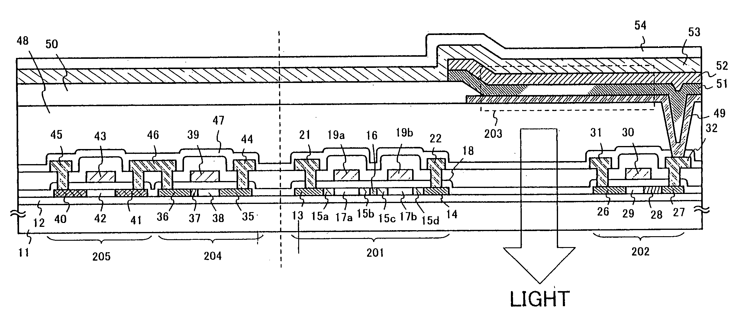
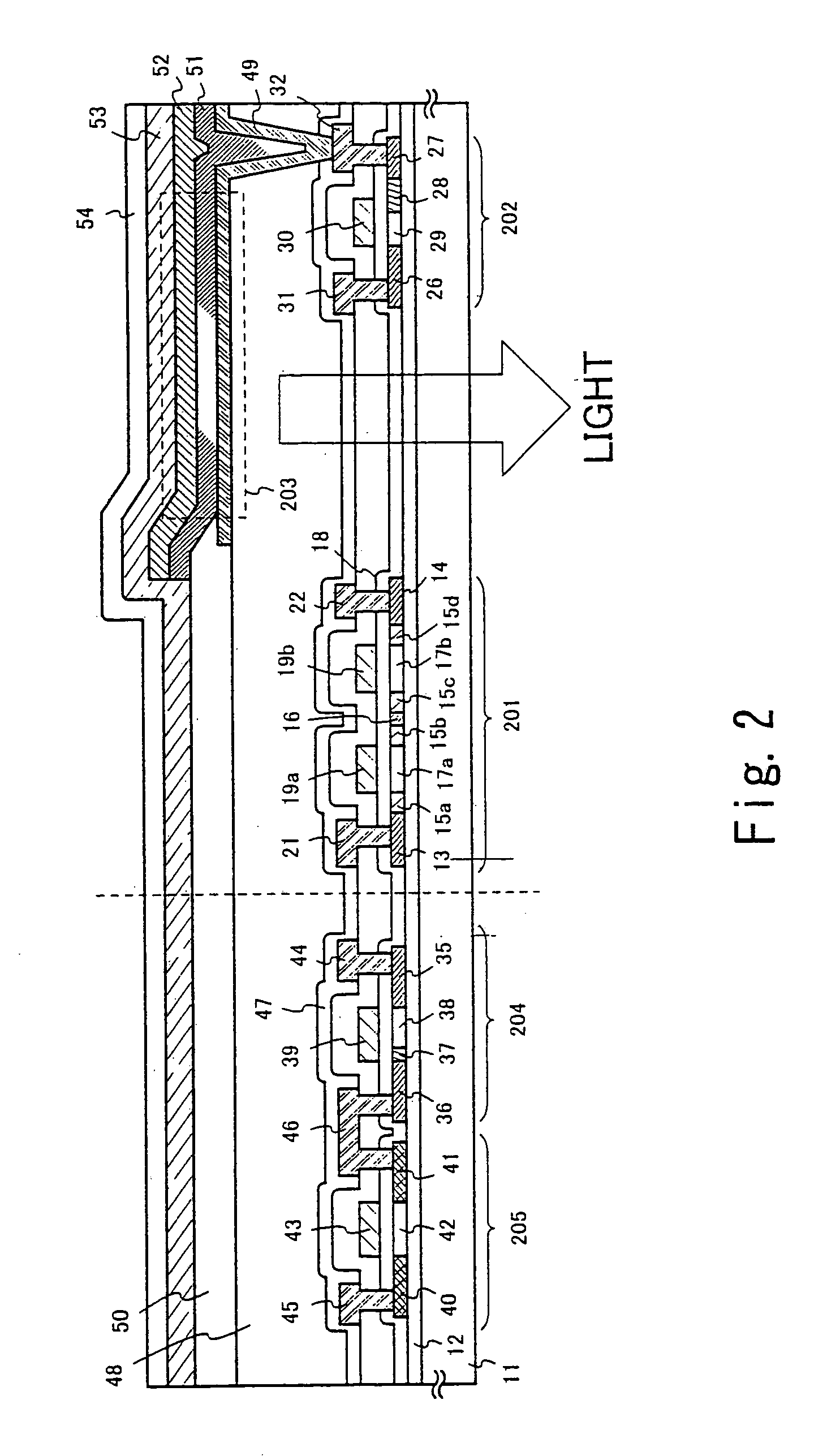
[0206] In this embodiment, the structure of a pixel different from that of FIG. 1(B) is shown in FIG. 14.

[0207] In this embodiment, the two pixels shown in FIG. 1(B) are arranged to be symmetrical with respect to the current-feed line 110 for giving earth potential. That is, the current-feed line 110 is made common to the two adjoining pixels, as shown in FIG. 14, and thereby the number of required wiring lines is decreased. There is no need to change the structure of TFTs disposed in the pixels.

[0208] This arrangement makes it possible to manufacture an even finer pixel portion, and improve the quality of an image.

[0209] In addition, the common structure of the current-feed line 110 makes it possible to expand the line width of the current-feed line 110 without the brightness of an image falling because the margin of the line width of the current-feed line 110 increases. Thus, the influence of a voltage drop of the current-feed line 110 can be reduced, and the voltage supplied f...

embodiment 3

[0211] In this embodiment, a description of forming a pixel portion having a structure different from that of FIG. 1 is given with reference to FIG. 15. The same steps as in embodiment 1 can be followed up to the step for forming the second interlayer insulating film 48. The switching TFT 201 covered with the second interlayer insulating film 48 and the current controlling TFT 202 each have the same structure as in FIG. 1, and a description thereof is omitted here.

[0212] In this embodiment, contact holes are made in the second interlayer insulating film 48 and the first passivation film 47, and then the pixel electrode 61 is formed. A 200 nm-thick aluminum alloy film (aluminum film that contains titanium of 1 wt %) is disposed as the pixel electrode 61 in this embodiment. Any material can be used as the pixel electrode on the condition that it is metallic. Preferably, it has a high reflectance.

[0213] The third interlayer insulating film 62 made of a silicon oxide film is formed th...


PUM

PropertyMeasurementUnit
spot diameteraaaaaaaaaa
thicknessaaaaaaaaaa
oscillation frequencyaaaaaaaaaa

Abstract

An EL display device capable of performing clear multi-gradation color display and electronic equipment provided with the EL display device are provided, wherein gradation display is performed according to a time-division driving method in which the luminescence and non-luminescence of an EL element (109) disposed in a pixel (104) are controlled by time, and the influence by the characteristic variability of a current controlling TFT (108) is prevented. When this method is used, a data signal side driving circuit (102) and a gate signal side driving circuit (103) are formed with TFTs that use a silicon film having a peculiar crystal structure and exhibit an extremely high operation speed.

Description

BACKGROUND OF THE INVENTION [0001] 1. Field of the Invention [0002] This invention relates to an EL (electro-luminescence) display device formed by constructing a semiconductor device (i.e., a device made of a semiconductor thin film) on a substrate and relates to electronic equipment (electronic device) in which the EL display device is used as a display panel (display portion). [0003] 2. Description of Related Art [0004] In recent years, great advances have been made in a technique for forming TFTs on a substrate, and development has proceeded in the application thereof to an active matrix type display. Especially, a TFT using a polysilicon film is higher in electron field-effect mobility than a conventional TFT using an amorphous silicon film, and can operate at a high speed. Therefore, it has been made possible to control a pixel by a driving circuit formed on the same substrate on which the pixel is also formed, although the pixel had been conventionally controlled by the drivi...

Claims


Application Information

Patent Timeline
Patent Type & Authority Applications(United States)
IPC IPC(8): G02F1/136H01L51/50G09F9/30H05B44/00G09G3/20G09G3/30H01L21/336H01L21/77H01L27/15H01L27/32H01L29/04H01L29/06H01L29/786H01L51/52H05B33/14H05B33/22H05B33/26
CPCG09G3/2018G09G3/2022H01L2924/0002G09G3/32G09G3/3258G09G2300/0417G09G2300/0842H01L27/1277H01L27/1296H01L27/156H01L27/3244H01L27/3246H01L27/3262H01L29/045H01L29/0603H01L29/78621H01L29/78624H01L29/78627H01L51/529H01L2251/5315H01L29/786H01L33/62G09G3/30G09G2300/023G09G2300/0408H01L2924/00H10K59/122H10K59/12H10K59/1213H10K50/87H10K2102/3026G02F1/136G09G3/3225G09G2300/04G09G2300/0426
Inventor YAMAUCHI, YUKIOFUKUNAGA, TAKESHI
Owner SEMICON ENERGY LAB CO LTD
Why Eureka
Try Eureka