Transistor and method for manufacturing the transistor

a transistor and semiconductor technology, applied in the field of transistors, can solve the problems of increasing drain electrode layer, and achieve the effect of reducing the characteristic variation of transistors, reducing the contact resistance between the oxide semiconductor layer and the source electrode layer and the drain electrode layer

Active Publication Date: 2010-08-05
SEMICON ENERGY LAB CO LTD
View PDF14 Cites 138 Cited by
  • Summary
  • Abstract
  • Description
  • Claims
  • Application Information

AI Technical Summary

Benefits of technology

[0026]In a transistor where an oxide semiconductor is used for a channel layer, in a region of an oxide semiconductor layer, a channel formation region between a source electrode layer and a drain electrode layer is formed to include an amorphous structure, and a region which is electrically connected to an external portion is formed to include a crystal structure. Thus, characteristic variation among transistors can be reduced and contact resistance between the oxide semiconductor layer and the source electrode layer and the drain electrode layer can be reduced.

Problems solved by technology

Meanwhile, in a case where an oxide semiconductor layer including an amorphous structure is used for a channel layer, there is a problem in that contact resistance between the oxide semiconductor layer and a source and a drain electrode layer is increased.

Method used


Image

  • Transistor and method for manufacturing the transistor
  • Transistor and method for manufacturing the transistor
  • Transistor and method for manufacturing the transistor

Examples


embodiment 1

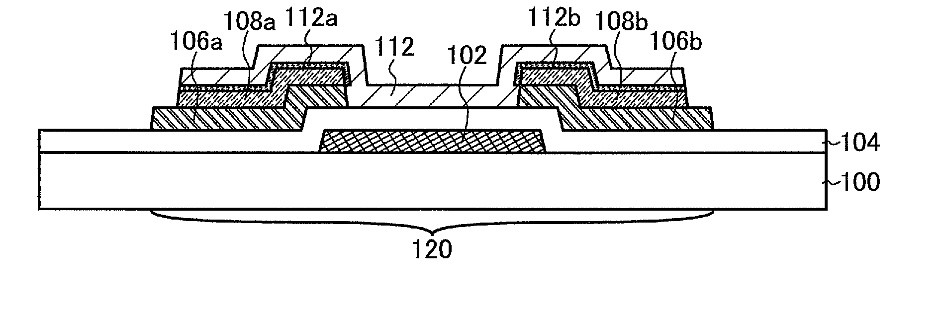
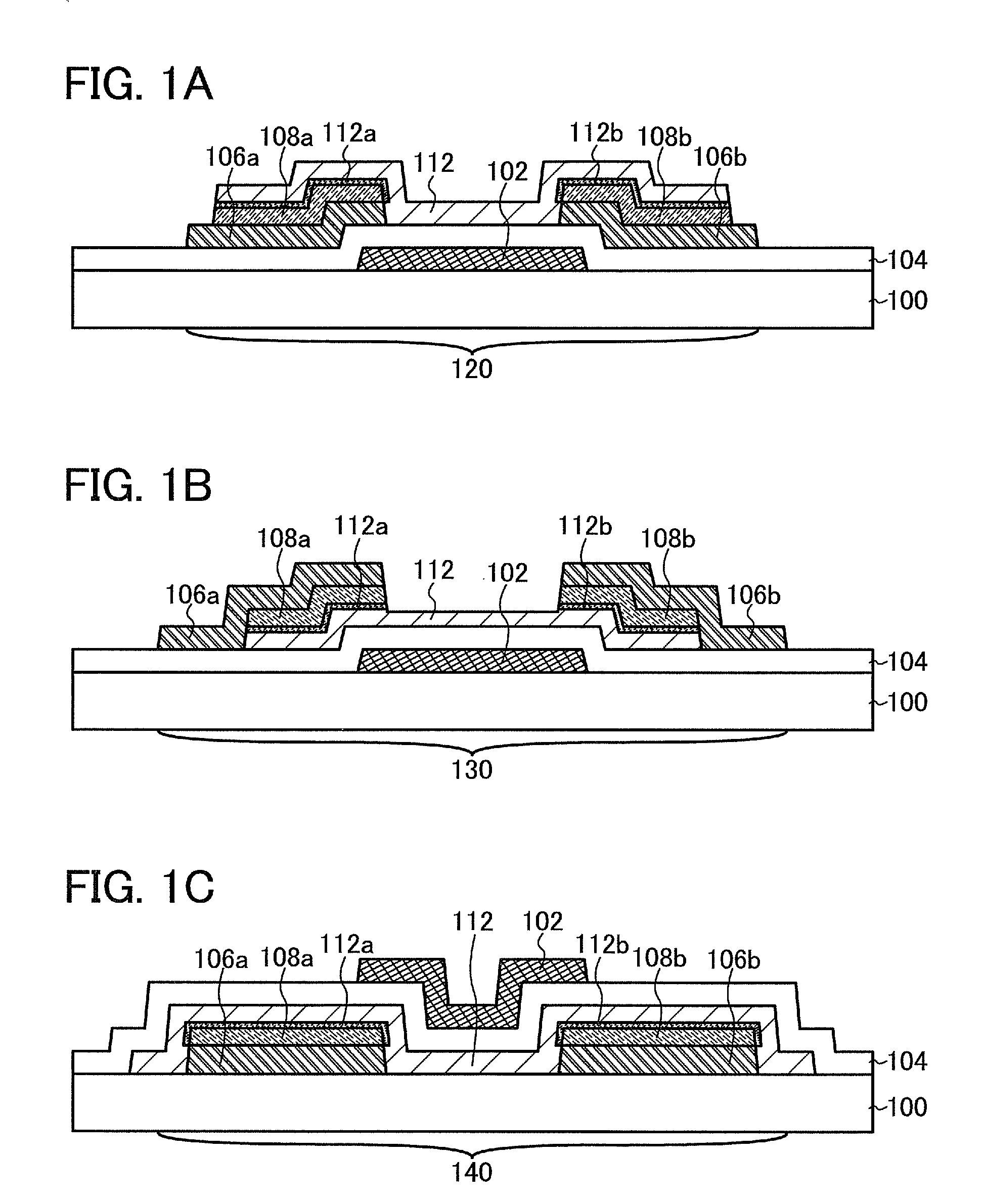
[0050]In this embodiment, examples of a structure of a transistor are described with reference to FIGS. 1A to 1C.

[0051]A transistor described in this embodiment includes a gate electrode 102, a gate insulating layer 104, a source electrode layer 106a, a drain electrode layer 106b, a first metal oxide layer 108a electrically connected to the source electrode layer 106a, a second metal oxide layer 108b electrically connected to the drain electrode layer 106b, and an oxide semiconductor layer 112 to be a channel layer. The oxide semiconductor layer 112 is provided in a region which overlaps with the gate electrode 102 with the gate insulating layer 104 interposed therebetween and is between the source electrode layer 106a and the drain electrode layer 106b. In addition, the oxide semiconductor layer 112 is provided in contact with the first metal oxide layer 108a and the second metal oxide layer 108b.

[0052]In the oxide semiconductor layer 112 to be a channel layer, a crystal structure...

embodiment 2

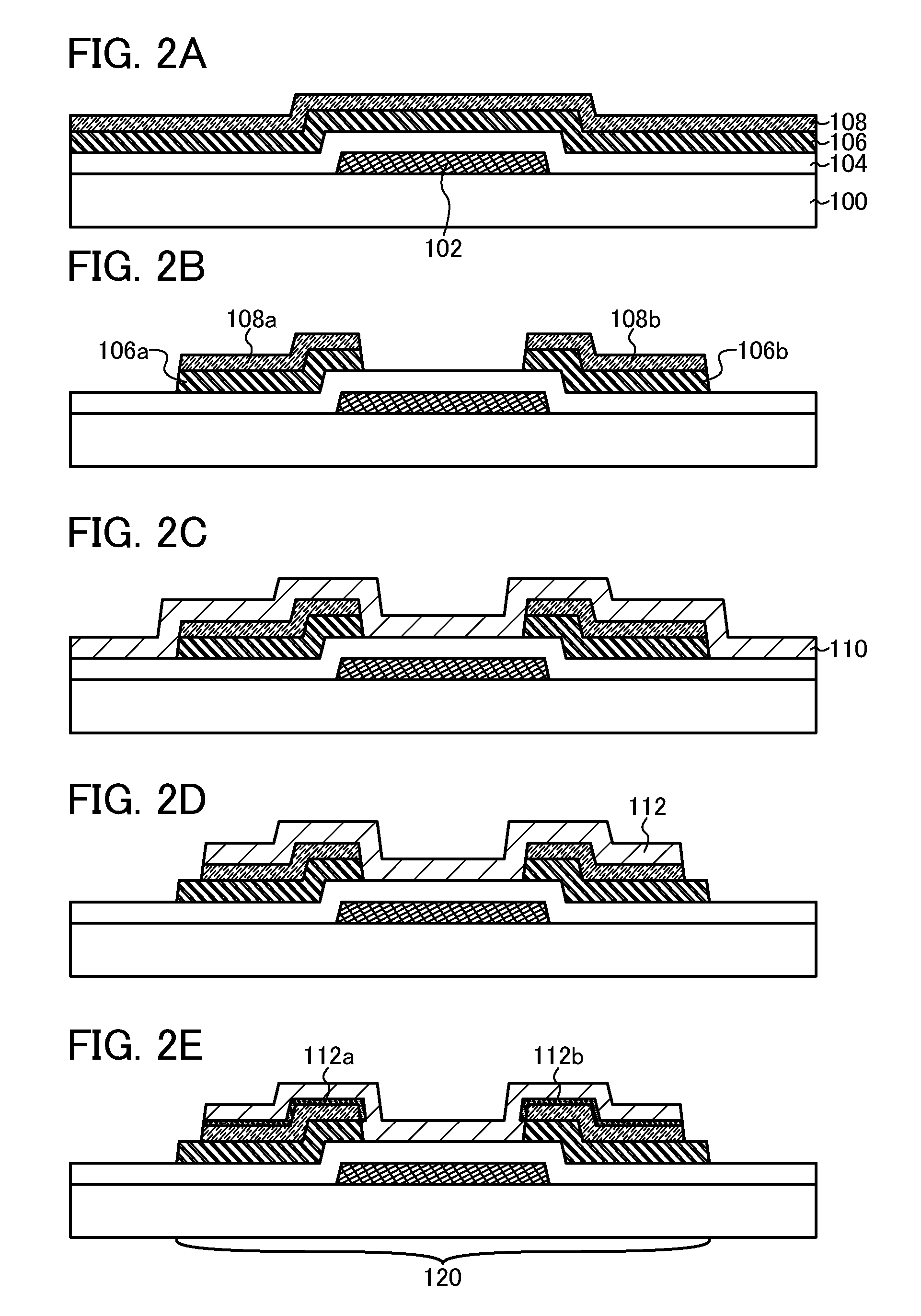
[0071]In this embodiment, an example of a manufacturing method in a case of using a bottom-gate transistor in the structure described in Embodiment 1 (the case illustrated in FIG. 1A) is described with reference to drawings.

[0072]First, the gate electrode 102 is formed over the substrate 100, and subsequently, the gate insulating layer 104 is formed over the gate electrode 102. Then, the conductive film 106 and the metal oxide layer 108 are sequentially stacked over the gate insulating layer 104 (see FIG. 2A).

[0073]As the substrate 100, a substrate having an insulating surface may be used, and for example, a glass substrate can be used. In addition, as the substrate 100, an insulating substrate formed using an insulator such as a ceramic substrate, a quartz substrate, or a sapphire substrate; a semiconductor substrate which is formed using a semiconductor material such as silicon and whose surface is covered with an insulating material; or a conductive substrate which is formed usin...

embodiment 3

[0127]In this embodiment, an example of a manufacturing method in a case of using a bottom-gate transistor in the structure described in Embodiment 1 (the case illustrated in FIG. 1B) is described with reference to drawings. Note that the manufacturing process (a material and the like which can be used) described in this embodiment has a lot in common with that described in Embodiment 2. Thus, description of the common portions is omitted, and different portions are described in detail below.

[0128]First, the gate electrode 102 is formed over the substrate 100, and subsequently, the gate insulating layer 104 is formed over the gate electrode 102. Then, the oxide semiconductor layer 110 and the metal oxide layer 108 are sequentially stacked over the gate insulating layer 104 (see FIG. 5A).

[0129]The oxide semiconductor layer 110 and the metal oxide layer 108 can be successively formed without exposure to the air. For example, after the oxide semiconductor layer 110 is formed by a sputt...


PUM


Abstract

It is an object to reduce characteristic variation among transistors and reduce contact resistance between an oxide semiconductor layer and a source electrode layer and a drain electrode layer, in a transistor where the oxide semiconductor layer is used as a channel layer. In a transistor where an oxide semiconductor is used as a channel layer, at least an amorphous structure is included in a region of an oxide semiconductor layer between a source electrode layer and a drain electrode layer, where a channel is to be formed, and a crystal structure is included in a region of the oxide semiconductor layer which is electrically connected to an external portion such as the source electrode layer and the drain electrode layer.

Description

BACKGROUND OF THE INVENTION[0001]1. Field of the Invention[0002]The present invention relates to a transistor using an oxide semiconductor layer, a semiconductor device provided with the transistor, and a method for manufacturing the same.[0003]2. Description of the Related Art[0004]Various metal oxides exist and are used for a variety of applications. Indium oxide is a well-known material and is used as a transparent electrode material which is necessary for liquid crystal displays and the like.[0005]Some metal oxides exhibit semiconductor characteristics. As metal oxides exhibiting semiconductor characteristics, tungsten oxide, tin oxide, indium oxide, zinc oxide, and the like are given. A thin film transistor in which such metal oxide exhibiting semiconductor characteristics is used for a channel formation region is disclosed (Patent Documents 1 to 4 and Non-Patent Document 1).[0006]As metal oxides, multi-component oxides are known as well as single-component oxides. For example,...

Claims


Application Information

Patent Timeline
Patent Type & Authority Applications(United States)
IPC IPC(8): H01L29/786H01L29/24H01L21/04H01L21/336
CPCH01L29/7869H01L27/1225H01L29/04
Inventor SAKATA, JUNICHIRO
Owner SEMICON ENERGY LAB CO LTD
Why Eureka
Try Eureka