Laminated magnetorestrictive element of an exchange coupling film, an antiferromagnetic film and a ferromagnetic film and a magnetic disk drive using same

a technology of antiferromagnetic film and ferromagnetic film, which is applied in the direction of nanoinformatics, magnetic bodies, instruments, etc., can solve the problems of high practical use problems, deterioration of the coupling field of the magnetoresistance effect film as a magnetoresistance element, and poor temperature characteristic of the exchange coupling field. achieve high mr ratio, efficient production of magnetoresistive elements, stable output voltage

Inactive Publication Date: 2001-11-06
KK TOSHIBA
View PDF17 Cites 139 Cited by
  • Summary
  • Abstract
  • Description
  • Claims
  • Application Information

AI Technical Summary

Benefits of technology

It is therefore an object of the present invention to eliminate the aforementioned problems and to provide a magnetoresistive element, wherein an exchange-coupling field between the antiferromagnetic film and a ferromagnetic film is sufficient or a low interlayer coupling between a pinned layer and a fre

Problems solved by technology

Since the magnetoresistance effect film of permalloy has magnetic domains, the Barkhausen noises resulting from this are much of a problem for practical use.
However, the .gamma.-FeMn alloy has the problem of corrosion resistance, particularly corrosion due to water, so that there is a problem in that the exchange coupling field to a magnetoresistance effect film as a magnetoresistive element is deteriorated by corrosion at a processing step or corrosion due to water in atmosphere as time elapses.
In addition, the temperature characteristic of the exchange coupling field is very bad.
Therefore, the exchange coupling field is not sufficient at 100.degree. C., so that there is a problem in that there is no long-term reliability.
However, these antiferromagnetic films are formed of Mn alloy which is difficult to prepare a high density target, so that it is difficult to manage the quality of the film.
However, when the antiferromagnetic underlies the ferroelectric film, there is a problem of the selection of the under layer that promotes a crystal growth.
However, although the above described spin valve structure can obtain a high output, there are problems in that there are some cases where the pinned layer is inverted by the electrostatic discharge (ESD) so that the output can be obtained, and that it is difficult to modify this to obtain the output again.
In addition, it is difficult to set the bias point of the element since a great bias magnetic field in the spin valve.
However, in the dual spin valve structure, it is not possible to obtain the output due to the variation in magnetic resistance unless the direction of the magnetization of the pinned layer is the same direction.
Therefore, there is a problem in that the method for modifying the inversion of the pinned layer for use in the conventional spin valve element can not be applied to the conventional dual spin valve structure.
On the other hand, in the dual spin valve structure, if the pinned layer is set so as to obtain a high output, a large bias magnetic field is produced from the pinned layer to the free layer, so that it is di

Method used


Image

  • Laminated magnetorestrictive element of an exchange coupling film, an antiferromagnetic film and a ferromagnetic film and a magnetic disk drive using same
  • Laminated magnetorestrictive element of an exchange coupling film, an antiferromagnetic film and a ferromagnetic film and a magnetic disk drive using same
  • Laminated magnetorestrictive element of an exchange coupling film, an antiferromagnetic film and a ferromagnetic film and a magnetic disk drive using same

Examples


example 2

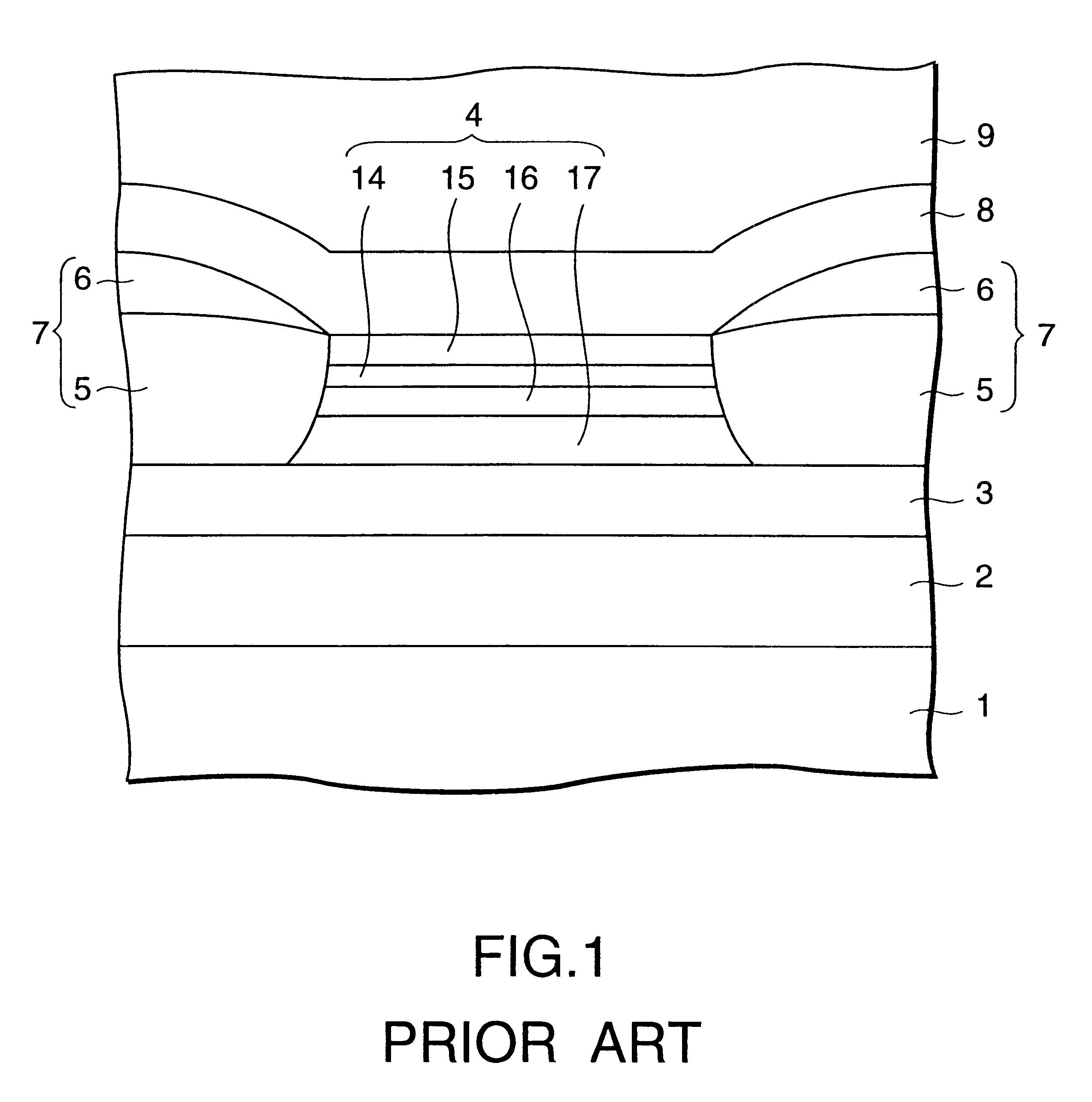
Using a DC magnetron sputtering system, the combinations of an antiferromagnetic film of IrMn and under layers of Ta (5 nm) / Au (2 nm), Ta (5 nm) / Ru (2 nm) and Ta (5 nm) / Ru (1 nm) / Au (1 nm) in the third preferred embodiment were prepared. With respect to these under layers, the dependencies of the MR ratio and the interlayer coupling on the thickness of IrMn were examined. The construction was under layer / IrMn / CoFe (2 nm) / Ru (0.9 nm) / CoFe (2 nm) / Cu (2 nm) / CoFe (2 nm) / Cu (1.5 nm) / Ta. As the cap layer, Cu was used. The results are shown in FIGS. 11 and 12. FIG. 11 shows the relationship between the thickness d (nm) of IrMn and the interlayer coupling field (Hin). FIG. 12 shows the relationship between the thickness d (nm) of IrMn and the MR ratio in each of the under layers. As can be seen from the drawings, the under layer of Ta / Au has a high MR ratio, and the under layer of Ta / Ru has a low interlayer coupling. Moreover, the under layer of Ta / Ru / Au has a high MR ratio and a low interl...

example 3

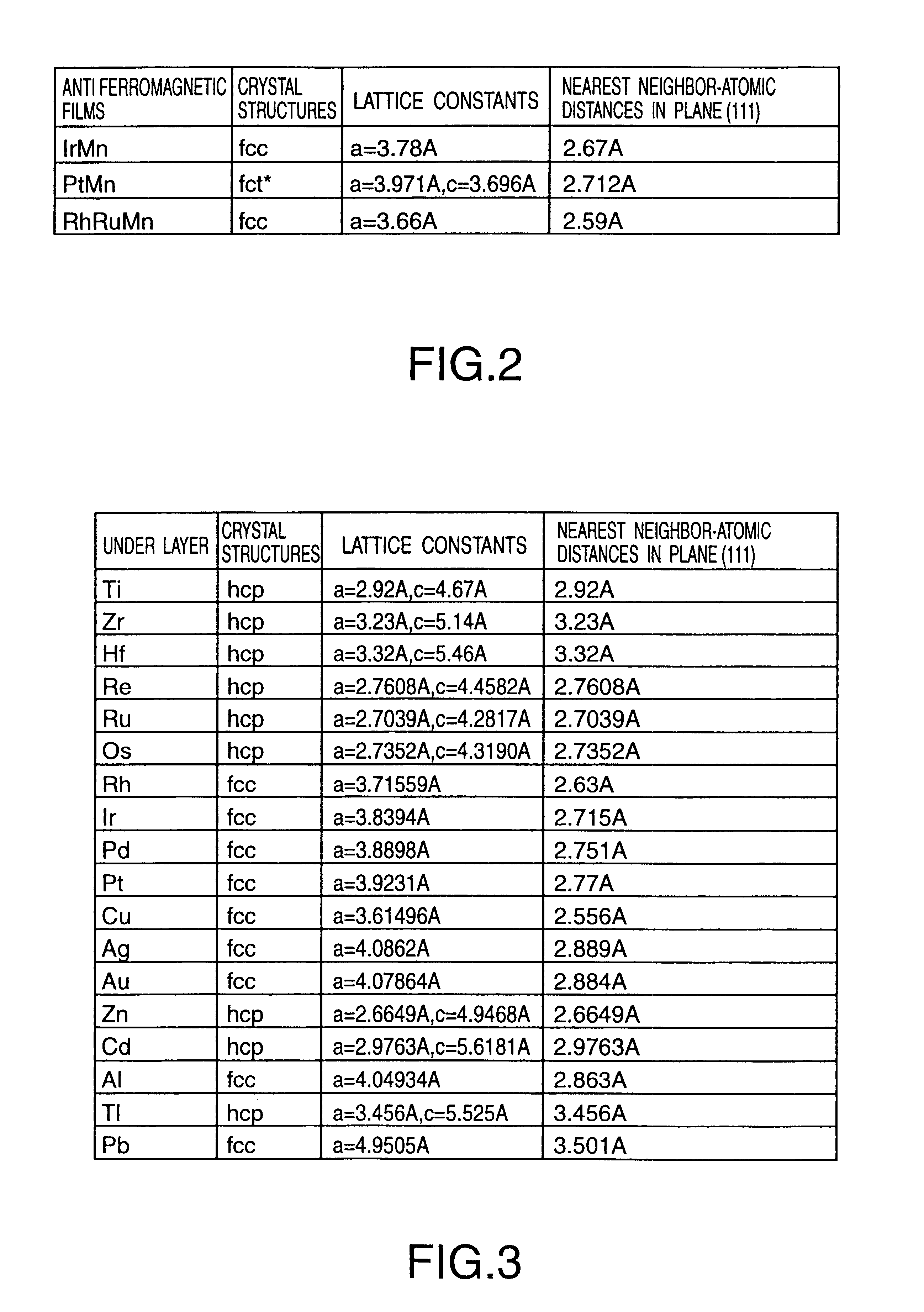
Using a DC magnetron sputtering system, the spin valve film in the third preferred embodiment was prepared. The antiferromagnetic films of IrMn and PtMn were used. At this time, Ta (5 nm) / Ru (1 nm) / NiFe (1 nm) was used as the under layer. As a result, when NiFe is combined with Ru, it was possible to obtain a low interlayer coupling field of 20 Oe or less and a high MR ratio. In addition, although the interlayer coupling field tends to increase as the thickness of the antiferromagnetic film increases, it was found that the dependence was small in the under layer of Ta (5 nm) / Ru (1 nm) / NiFe (1 nm). In addition, the same results were obtained even in the case of combinations of Rh, Ir, Cr, Re, Tc, Os other than Ru, and elements having a longer nearest neighbor atomic distance than that of the antiferromagnetic film. Moreover, with respect to NiFe, the same results were obtained even in the case of NiFe-X wherein a non-magnetizing element, such as NiFeCr, is added.

example 4

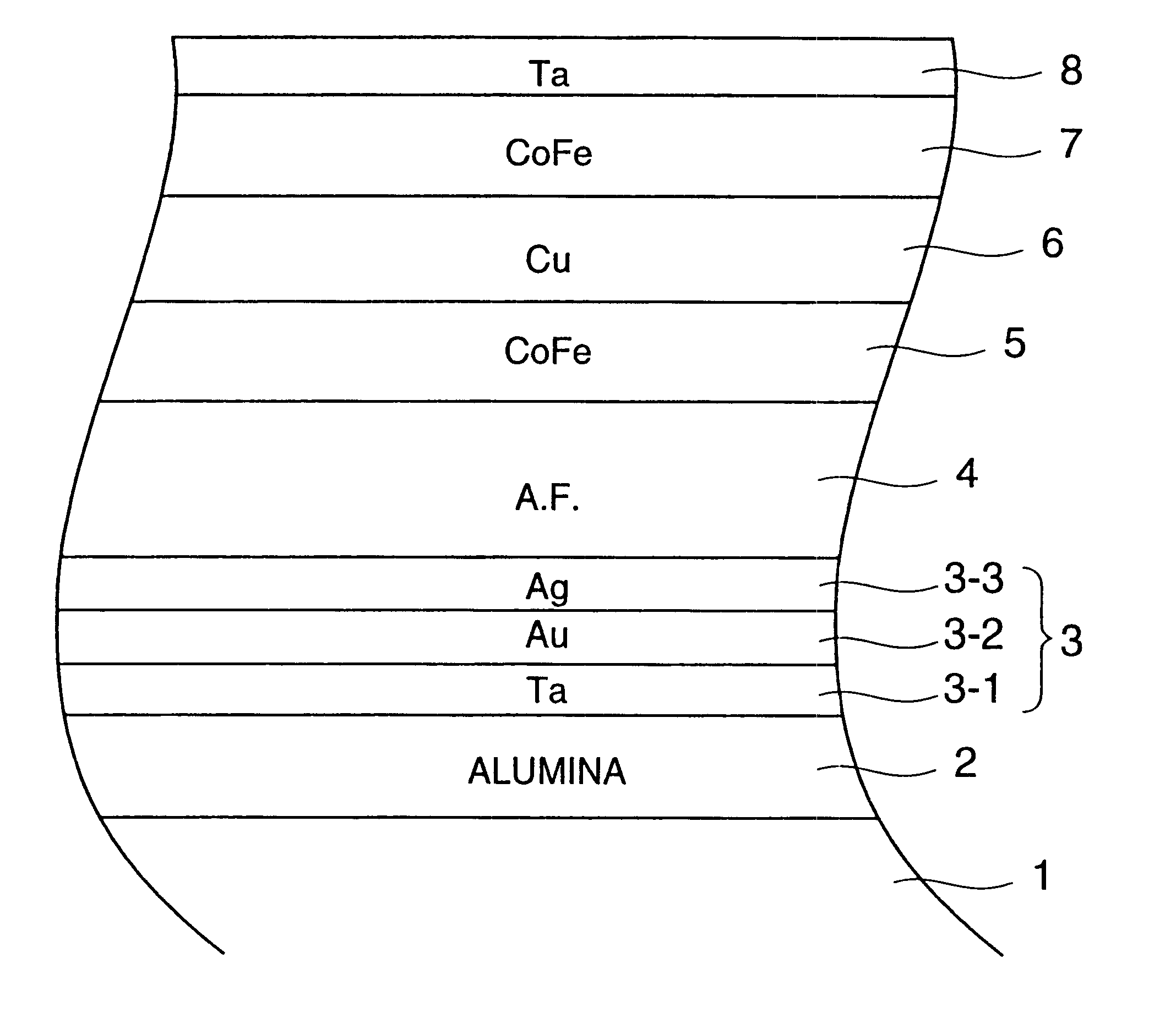
The following samples were prepared on alumina.

1 5Ta / 2Ru / 10PtMn / 2CoFe / 0.9Ru / 2.5CoFe / xCu / 2CoFe / 2Cu / 5Ta x=1.9, 2, 2.1, 2.2, 2.3, 2.4, 2.6

2 5Ta / 2NiFe / 10PtMn / 2CoFe / 0.9Ru / 2.5CoFe / xCu / 2CoFe / 2Cu / 5Ta x=1.8, 2, 2.1, 2.2, 2.3, 2.5, 2.7

3 5 Ta / 2Au / 10PtMn / 2CoFe / 0.9Ru / 2.5CoFe / xCu / 2CoFe / 2Cu / 5Ta x=1.8, 2, 2.1, 2.2, 2.3, 2.5, 2.8

All of the samples were annealed in a magnetic field of 7 kOe in vacuum of 10.sup.-6 Torr for 10 hours. All of the numbers have a unit nm.

FIG. 13 shows the results of the Hin.

The distribution of thickness of the Cu spacer estimated on the basis of these results was a normal distribution of standard deviation of about 25 im in the case of 1, and a normal distribution of standard deviation of about 0.2 nm in the case of 2. The components of the Hin based on the contribution of the magnetostatic coupling are substantially the same. However, the Ru under layer has a smaller variation due to the RKKY oscillation of the Hin in a region of from 2 nm to 2.5 nm, and the controllabili...


PUM


Abstract

A magnetoresistive element comprises an exchange coupling film having a under layer, an antiferromagnetic film and a ferromagnetic film, which are laminated in that order, the under layer including a metal having a face centered cubic crystal structure or hexagonal closest packing crystal structure which have a longer nearest neighbor atomic distance than that of the antiferromagnetic film. With this construction, it is possible to improve the exchange coupling field and to satisfy a stable output over a long period of time. A magnetoresistive element having a dual spin valve structure has a magnetization adjusting layer, which is antiferromagnetically connected to a pinned layer via an anti-parallel connection layer, to adjust the value of the product of the saturation magnetization of each of the magnetization adjusting layer and the pinned layer by the thickness thereof. Moreover, a magnetoresistance head use a giant magnetoresistance effect, and has at least one pair of pinned layer and free layer arranged via a non-magnetic spacer layer. The pinned layer has a pair of ferromagnetic layers which have different compositions and different coercive forces and which are antiferromagnetically connected to each other via a connection layer, so that the effective exchange coupling field of the pinned layer is 200 Oe or more.

Description

1. Field of the InventionThe present invention relates generally to a magnetoresistive element having an change coupling film utilizing an exchanging coupling between an antiferromagnetic film and a ferromagnetic film, a magnetic head using the magnetoresistive element, and a magnetic disk drive using the magnetic head.2. Description of the BackgroundAs a read head in a high density magnetic recording, a magnetic head using a magnetoresistive element has been studied. At present, an 80 at % Ni-20 at % Fe (coummn name: permalloy) alloy thin-film is used as a material of the magnetoresistive element. In recent years, as materials substituted for this, artificial lattice films and spin valve films, such as (Co / Cu)n, which have a giant magnetoresistance effect, are widely noticed.Since the magnetoresistance effect film of permalloy has magnetic domains, the Barkhausen noises resulting from this are much of a problem for practical use. Therefore, various methods for causing a magnetoresi...

Claims


Application Information

Patent Timeline
IPC IPC(8): G11B5/39H01F10/32H01F10/00G11B5/012
CPCB82Y10/00B82Y25/00G11B5/3903H01F10/3263H01F10/3268H01F10/3272G11B5/012G11B5/3967G11B2005/3996
Inventor FUKE, HIROMISAITO, KAZUHIROKOUI, KATSUHIKOFUKUZAWA, HIDEAKISAITO, AKIKOIWASAKI, HITOSHI
Owner KK TOSHIBA
Why Eureka
Try Eureka