Method and apparatus for cutting protective tape

a protective tape and tape cutting technology, applied in the direction of mechanical control devices, instruments, process and machine control, etc., can solve the problems of cutting blade tip being prone to be damaged by friction with respect to the wafer, contaminated pattern damage,

Inactive Publication Date: 2005-04-21
NITTO DENKO CORP
View PDF1 Cites 16 Cited by
  • Summary
  • Abstract
  • Description
  • Claims
  • Application Information

AI Technical Summary

Benefits of technology

[0031] With this configuration, the height of the cutter blade can be changed in accordance with the contact portion of the semiconductor wafer. That is, the cutter blade can be maintained such that a predetermined portion of the cutter blade is brought into contact with the semiconductor wafer.

Problems solved by technology

Herein, since stress caused by the grinding operation is applied to the surface of the wafer and there is a probability that the pattern is damaged or contaminated.
If the protective tape is cut in the state where the tip end of the cutter blade is brought into contact with the outer circumferential edge of the wafer, the tip end of the cutter blade is prone to be damaged by friction with respect to the wafer.
In this state, if the protective tape joined to the surface of the wafer is cut, there is a problem that viscoelastic particle component of the protective tape protrudes from the cut portion and the particles are attached to the outer circumferential edge of the wafer.

Method used


Image

  • Method and apparatus for cutting protective tape
  • Method and apparatus for cutting protective tape
  • Method and apparatus for cutting protective tape

Examples


Embodiment Construction

[0043] Hereinafter, description will be given of one example of embodiment of the present invention with reference to the drawings.

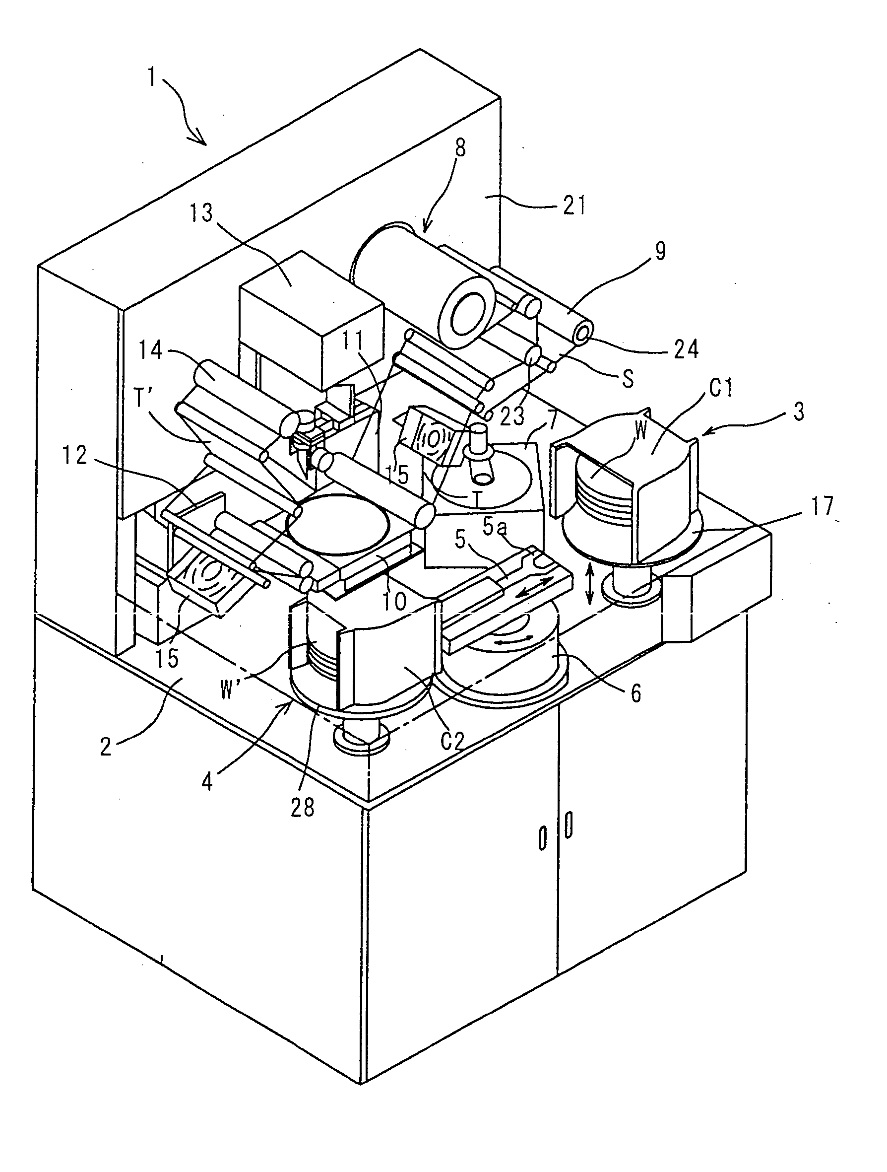
[0044]FIG. 1 is a perspective view showing a schematic configuration of a protective tape joining apparatus with which a protective tape cutting apparatus according to this embodiment is equipped.

[0045] This protective tape joining apparatus 1 includes a base 2. On the base 2, on the side of its front edge, there are provided a wafer supply unit 3 into which a cassette C1 is loaded, and a wafer collector 4 which collects a processed wafer W′. Semiconductor wafers W (hereinafter, simply referred to as “wafers W”) having orientation flats are contained in the cassette C1. A protective tape T is joined to a surface of the wafer W, and the protective tape T is cut. This wafer is called the processed wafer W′. A wafer transport mechanism 6 having a robot arm 5 is disposed between the wafer supply unit 3 and the wafer collector 4. An alignment stage 7 is dis...


PUM

PropertyMeasurementUnit
curvatureaaaaaaaaaa
thicknessaaaaaaaaaa
stressaaaaaaaaaa

Abstract

The present invention provides a method of moving a cutter blade along a circumferential edge of a semiconductor wafer, thereby cutting a protective tape joined to a surface of the semiconductor wafer with a pattern formed thereon for protecting the pattern before the semiconductor is processed. The cutter blade moves in the state where a side face thereof is brought into contact with the circumferential edge of the semiconductor wafer, thereby cutting the protective tape joined to the surface of the semiconductor wafer.

Description

BACKGROUND OF THE INVENTION [0001] (1) Field of the Invention [0002] The present invention relates to a technique for cutting, along a circumferential edge of a semiconductor wafer, a protective tape joined to a surface of the semiconductor wafer with a pattern formed thereon for protecting the pattern. [0003] (2) Description of the Related Art [0004] In a conventional producing procedure of a semiconductor wafer, a back surface of a semiconductor wafer (hereinafter, simply referred to as “wafer”) is worked using a mechanical method such as a grinding method and a polishing method (CMP) or a chemical method such as an etching method, thereby reducing a thickness of the wafer. When the wafer is worked using such a method, a protective tape is joined to a surface for protecting a pattern formed on the surface. [0005] That is, a surface (patterned surface) of a wafer transported to a back grind step is suction-held by a chuck table, and its back surface is ground by a grindstone. Herei...

Claims


Application Information

Patent Timeline
Patent Type & Authority Applications(United States)
IPC IPC(8): B26D3/10B26F1/38B29C63/02B65H35/06H01L21/00H01L21/304
CPCB26F1/3846B29C63/02B29C2793/00H01L21/67092H01L21/67132Y10T156/1734Y10T156/1348Y10T82/16016Y10T156/12Y10T156/1085Y10T82/16032Y10T156/1343Y10T156/108Y10T83/05B65H35/06
Inventor YAMAMOTO, MASAYUKI
Owner NITTO DENKO CORP
Why Eureka
Try Eureka