Manufacturing method of quartz crystal resonator, apparatus therefor, and quartz crystal resonator manufactured thereby

Active Publication Date: 2005-11-24
SEIKO EPSON CORP
View PDF10 Cites 17 Cited by
  • Summary
  • Abstract
  • Description
  • Claims
  • Application Information

AI Technical Summary

Benefits of technology

[0019] Also, in the above described method, the quartz crystal resonator to which a laser beam has applied is immersed in a corrosive liquid. Thus the processing dust that is adherent to the surface of a quartz crystal resonator by application of the laser beam is removed and therefore the performance of a quartz crystal resonator improves. The corrosive liquid is hydrofluoric acid, ammonium fluoride, buffered hydrogen fluoride, Max7011G, ammonium bifluoride, or an alkaline liquid at least including potassium hydroxide.
[0020] An apparatus for manufacturing a quartz crystal resonator according to the present invention comprises a laser oscillator for emitting a laser beam that is absorbed inside a crystal chip and a movement mechanism for moving the laser oscillator for a predetermined pitch, wherein the laser beam is applied to an end of the crystal chip while the movement mechanism moves the laser oscillator from the vicinity of the end towards the end for a predetermined pitch such that a step section having a plurality of steps are formed. The present invention makes it easy to control the shape of a quartz crystal resonator even if the quartz crystal resonator is miniaturized, makes the shape and the performance of a processed quartz crystal resonator satisfactory, can form quartz crystal resonators of various shapes, can form a quartz crystal resonator at low cost with a small number of man-hours, has a small load in driving a quartz crystal resonator, and can use versatile equipment and tools.
[0021] An apparatus for manufacturing a quartz crystal resonator accordin

Problems solved by technology

The above described first conventional example has problems that controlling its shape becomes difficult as an AT cut quartz crystal resonator is miniaturized and roughness of a surface of an AT cut quartz crystal wafer and a degenerated layer occur due to the use of blasting, which sprays fine abrasives to break an AT cut quartz crystal wafer.
The above described second conventional example also has, in addition to the same problems as mentioned for the first conventional example, a problem that the example can be applied just to the disk shaped AT cut quartz crystal resonators and therefore the versatility is low.
In the above described third conventional example, there are problems that the formation of an electrode having a stair-like and angled structure takes a large number of man-

Method used


Image

  • Manufacturing method of quartz crystal resonator, apparatus therefor, and quartz crystal resonator manufactured thereby
  • Manufacturing method of quartz crystal resonator, apparatus therefor, and quartz crystal resonator manufactured thereby
  • Manufacturing method of quartz crystal resonator, apparatus therefor, and quartz crystal resonator manufactured thereby

Examples


first embodiment

[0034] First Embodiment

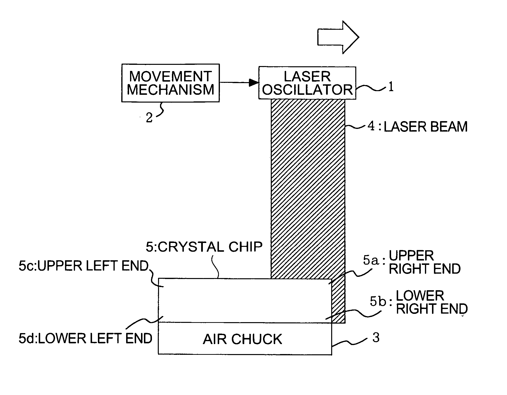
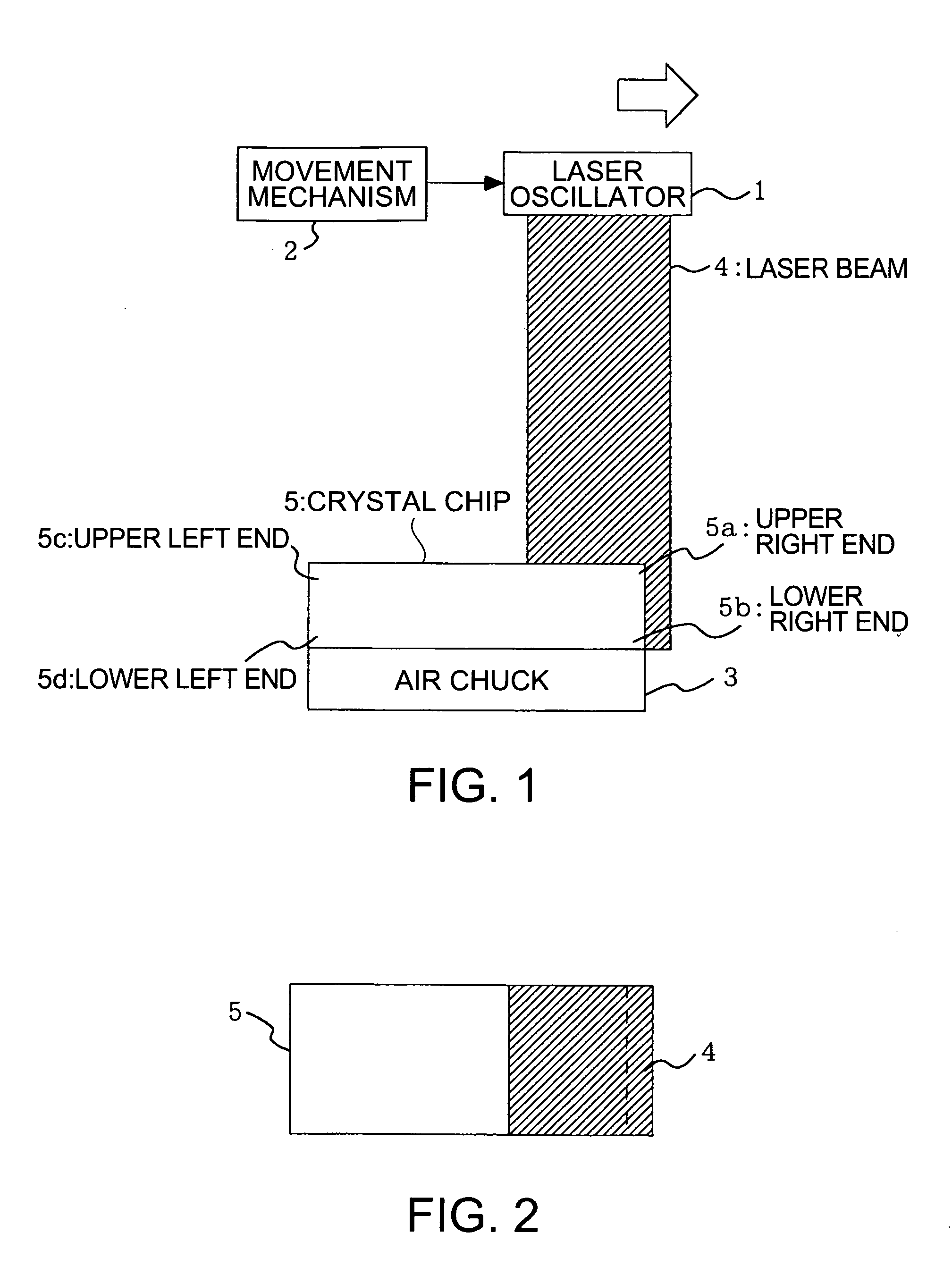
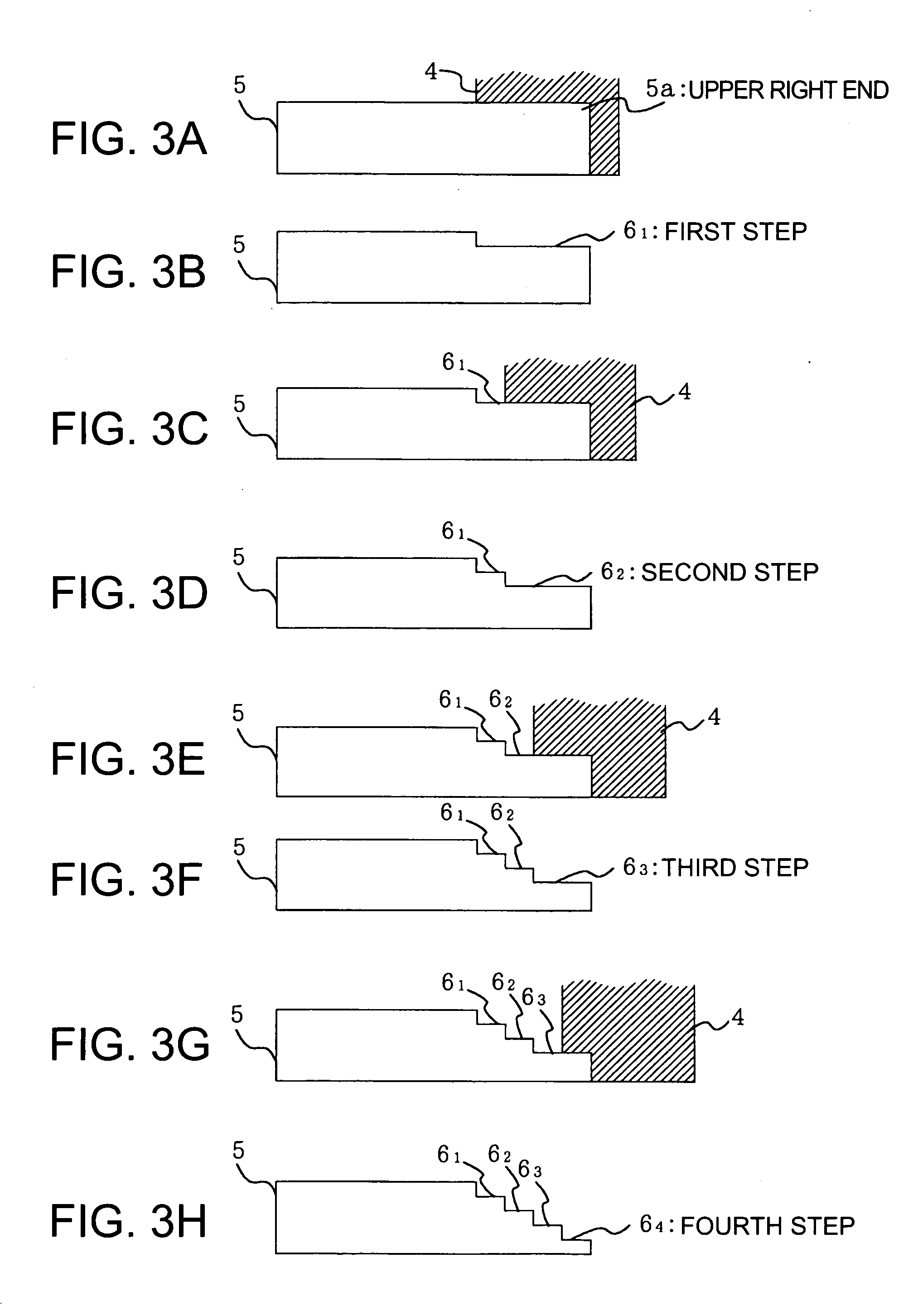
[0035]FIG. 1 is a schematic diagram showing a structure of an apparatus for manufacturing a quartz crystal resonator that is a first embodiment of the present invention. The apparatus for manufacturing a quartz crystal resonator in this example generally comprises a laser oscillator 1, a movement mechanism 2, and an air chuck 3. The laser oscillator 1 is, for example, a F2 laser (fluorine) and oscillates to emit a laser beam 4 having 157 nm wavelength and uniform intensity distribution. The radiation pattern of the laser beam 4 is rectangular as shown in FIG. 2. The reason of employing the F2 laser in this example is that a laser beam emitted from the F2 laser is absorbed into a crystal chip 5 that is a transparent material thereby enabling processing. Accordingly, a laser that emits a laser beam to be absorbed into the crystal chip 5, thereby enabling processing, is accepted as the laser oscillator 1. As another laser than the F2 laser, for example, an ultra ...

second embodiment

[0044] Second Embodiment

[0045]FIG. 5 is a plan view of a mask 21 used in a manufacturing apparatus of a quartz crystal resonator that is a second embodiment of the present invention. The structure of the apparatus, except the mask 21, is the same as that shown in FIG. 1. The mask 21, as shown in FIG. 5, has an approximately shape with the width slightly larger than that of the crystal chip 5 to be processed and the length that is around half the length of the crystal chip 5. In the mask 21, a light shielding film 21a that contains a transmission section 21b with four sides is formed on a glass plate. Three sides of the transmission section 21b that are adjacent one another are made of straight lines. The remaining one side, namely the side that is located on the center side of the crystal chip 5 when the mask is placed on the crystal chip 5, has a circular arc shape such that the transmission section 21b is concave at the center side of the crystal chip 5. The light shielding film 2...

third embodiment

[0050] Third Embodiment

[0051] Each of the above embodiments shows the example of fixing the crystal chip 5 and moving the side of the laser oscillator 1 or the side of the laser oscillator 1 and the mask 21, but the present invention is not restricted to this example. For example, an embodiment may be structured such that the side of the laser oscillator 1 is fixed while the crystal chip 5 or the side of the crystal chip 5 on which the mask 21 is placed is moved in the opposite direction to the arrow direction shown in FIG. 1 by an XY stage or the like.


PUM

PropertyMeasurementUnit
Heightaaaaaaaaaa

Description

RELATED APPLICATIONS [0001] This application claims priority to Japanese Patent Application Nos. 2004-151475 filed May 21, 2004 and 2005-000411 filed Jan. 5, 2005 which are hereby expressly incorporated by reference herein in their entirety. BACKGROUND [0002] 1. Technical Field [0003] The present invention relates to a manufacturing method of a quartz crystal resonator for manufacturing an AT cut quartz crystal resonator having a convex sectional shape by processing a crystal chip, an apparatus for the method, and a quartz crystal resonator manufactured by this manufacturing method or this manufacturing apparatus. [0004] 2. Related Art [0005] In a conventional method for manufacturing a piezoelectric resonator, blasting is applied to either or both of an AT cut quartz crystal wafer by spraying fine abrasives from a nozzle with a small bore onto desired narrow ranges at both sides along visible outlines of a piezoelectric element piece, thereby manufacturing a piezoelectric element p...

Claims


Application Information

Patent Timeline
IPC IPC(8): H02N2/00H03H3/02H03H9/19
CPCH03H3/02Y10T29/42H03H2003/0435H03H9/19
Inventor UMETSU, KAZUSHIGE
Owner SEIKO EPSON CORP
Why Eureka
Try Eureka