Method of forming a CMOS transistor

Active Publication Date: 2005-04-21
AU OPTRONICS CORP
View PDF3 Cites 2 Cited by
  • Summary
  • Abstract
  • Description
  • Claims
  • Application Information

AI Technical Summary

Benefits of technology

[0012] It is therefore an object of the invention to provide a manufacturi

Problems solved by technology

However, each manufacturing procedure adds to an increase in manufacturing cost.

Method used


Image

  • Method of forming a CMOS transistor
  • Method of forming a CMOS transistor
  • Method of forming a CMOS transistor

Examples


Embodiment Construction

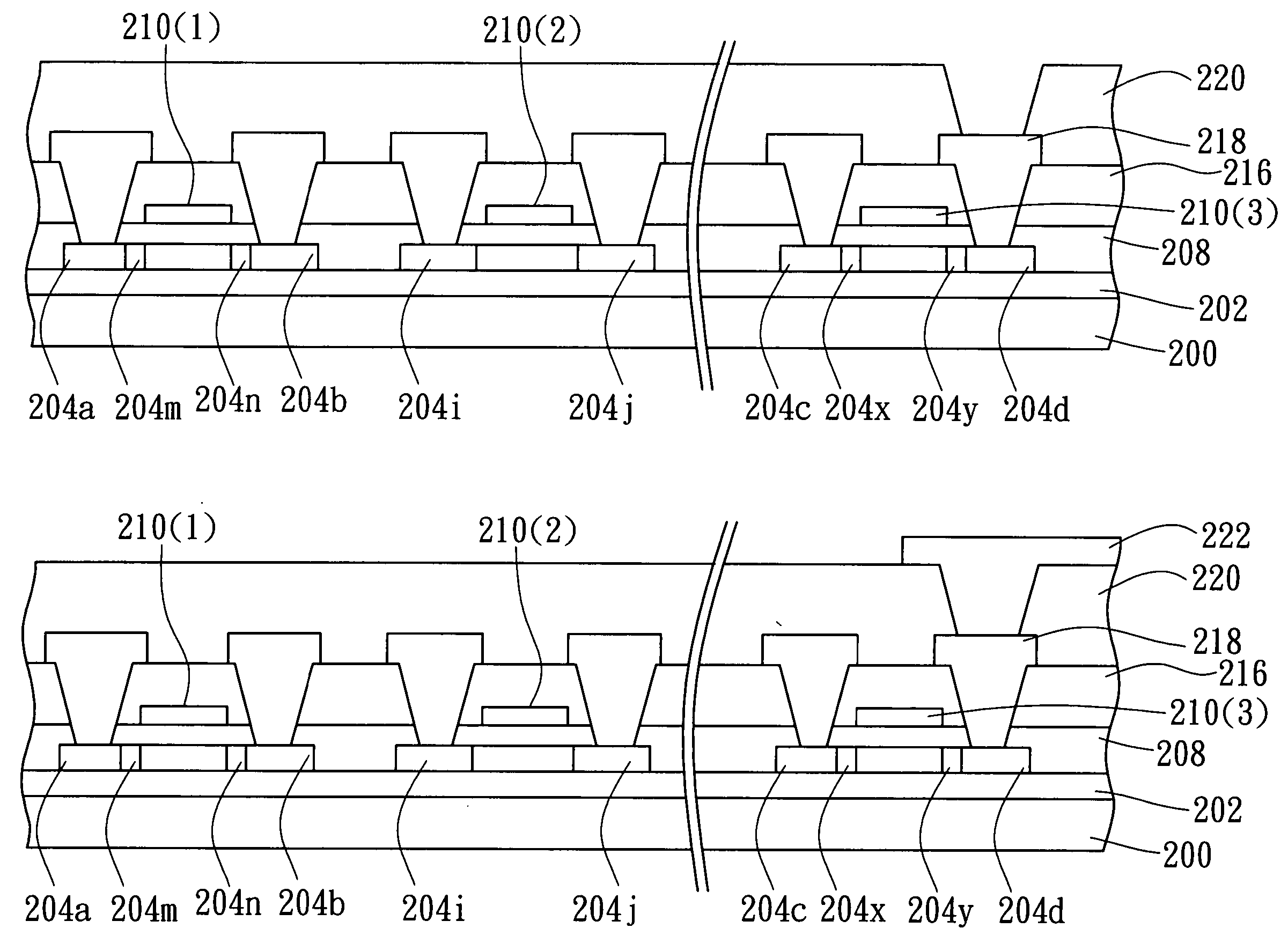
[0020] The invention provides a manufacturing process of low-temperature polysilicon thin film transistor with fewer steps.

[0021] Referring to FIG. 2A˜2H, these diagrams show the manufacturing process of a low-temperature polysilicon thin film transistor suitable for liquid crystal display (LCD) according to the invention. First of all, in FIG. 2A, a buffer layer 202 and a polysilicon layer are sequentially formed on a substrate 200. Next, a patterned photoresist layer (not shown here) is formed on the polysilicon layer, and the photoresist layer is used as a shield during etching process to form a polysilicon layer 204(1), 204(2), and 204(3) shown in FIG. 2A.

[0022] Substrate 200 according to the invention can be made of glass or plastics. Polysilicon layer 204(1), 204(2), and 204(3) with the thickness of about 200˜1000 angstroms are formed by crystallization annealing an amorphous silicon layer on buffer layer 202 by using excimer laser. The polysilicon layers 204(1) and 204(2) a...


PUM


Abstract

A method of forming a CMOS transistor on a substrate is provided, wherein the method requires only two implanting procedures to form all source / drain and light doped region. First, the source / drain of an NMOS transistor is formed by using a photoresist layer which covers up the source / drain of a PMOS transistor as a mask with a phosphorus dopant being implanted into. Next, the lightly doped region of an NMOS transistor and the source / drain of a PMOS transistor are formed by using a photoresist layer which covers up the source / drain of an NMOS transistor as well as the gate as masks with a boron dopant being implanted into. Of which, the dosage of the boron dopant is smaller than that of the phosphorus dopant.

Description

[0001] This application claims the benefit of Taiwan application Serial No. 92128630, filed Oct. 15, 2003. BACKGROUND OF THE INVENTION [0002] 1. Field of the Invention [0003] The invention relates in general to a manufacturing method of forming a CMOS transistor, and more particularly to a manufacturing method of forming the source / drain and lightly doped region of a CMOS transistor using two procedures of implantation. [0004] 2. Description of the Related Art [0005] While most thin film transistors used in flat displays are manufactured via amorphous silicon manufacturing process, only a few advanced products adopt polysilicon manufacturing process which has higher electron mobility. Polysilicon technology allows more electronic circuits to be integrated into, so the overall complexity and weight of product can be reduced. Since the highest temperature during polysilicon manufacturing process is over 3000° C., a temperature far above the softening point of plastics, so this manufac...

Claims


Application Information

Patent Timeline
IPC IPC(8): H01L21/20H01L21/77H01L21/8238H01L21/84
CPCH01L27/1214H01L27/127H01L27/1288
Inventor CHEN, KUN-HONGCHEN, MING-YAN
Owner AU OPTRONICS CORP
Why Eureka
Try Eureka