Printed circuit board with low noise

a printed circuit board and low noise technology, applied in the direction of cross-talk/noise/interference reduction, line-transmission details, electrical apparatus construction details, etc., can solve problems such as different signals, and achieve the effect of reducing noise within the printed circuit board and low nois

Inactive Publication Date: 2005-05-05
TATUNG COMPANY
View PDF4 Cites 18 Cited by
  • Summary
  • Abstract
  • Description
  • Claims
  • Application Information

AI Technical Summary

Benefits of technology

[0007] A main objective of the present invention is to provide a printed circuit board with low noise that can reduce noise within the printed circuit board.

Problems solved by technology

Furthermore, different signals can interfere with each other due to electro-magnetic coupling generated by the signal lines crossing the isolation area of the printed circuit board, and the electro-magnetic radiation may exceed a predetermined maximum.

Method used


Image

  • Printed circuit board with low noise
  • Printed circuit board with low noise
  • Printed circuit board with low noise

Examples


Embodiment Construction

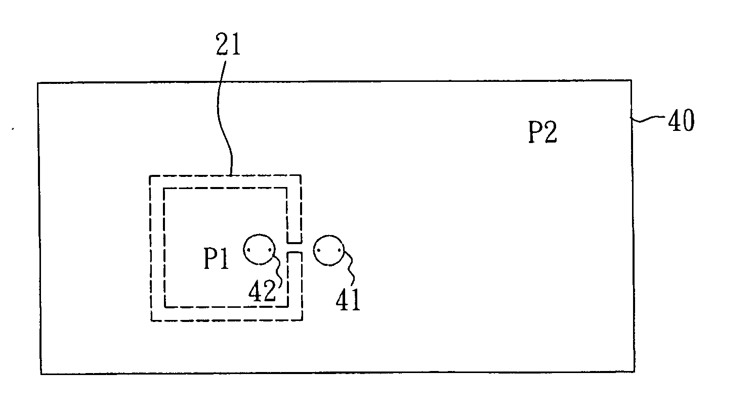
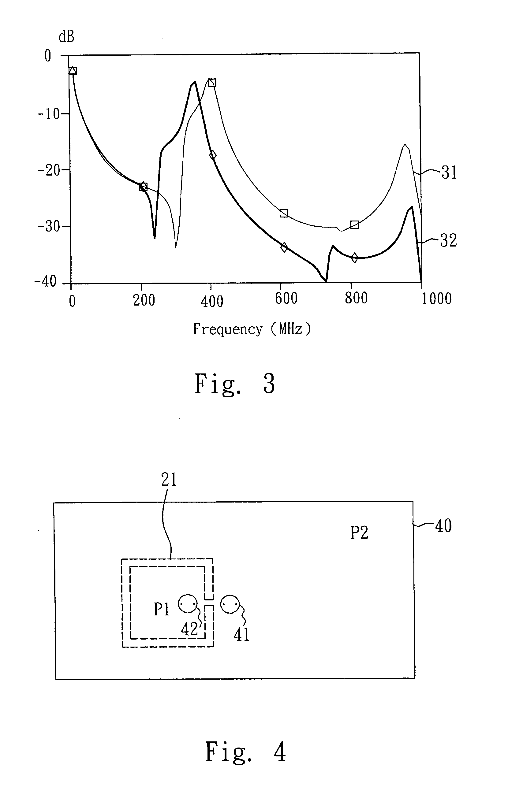
[0016] The printed circuit board with low noise in the present invention utilizes an isolation line to divide the printed circuit board into two areas: an analog area and a digital area. Since the digital area is not a closed area, the analog area and the digital area can be electrically connected and have the same voltage level. At least one capacitor is placed near the opening (only on one side or either sides of the opening) between the analog area and the digital area, and is utilized to remove noise by capacitive filtering effects. When the signal line running across the opening between the analog area and the digital area with identical power reference voltage level, the signal quality on the signal line will be maintained, and the electro-magnetic radiation of the printed circuit board can also be reduced.

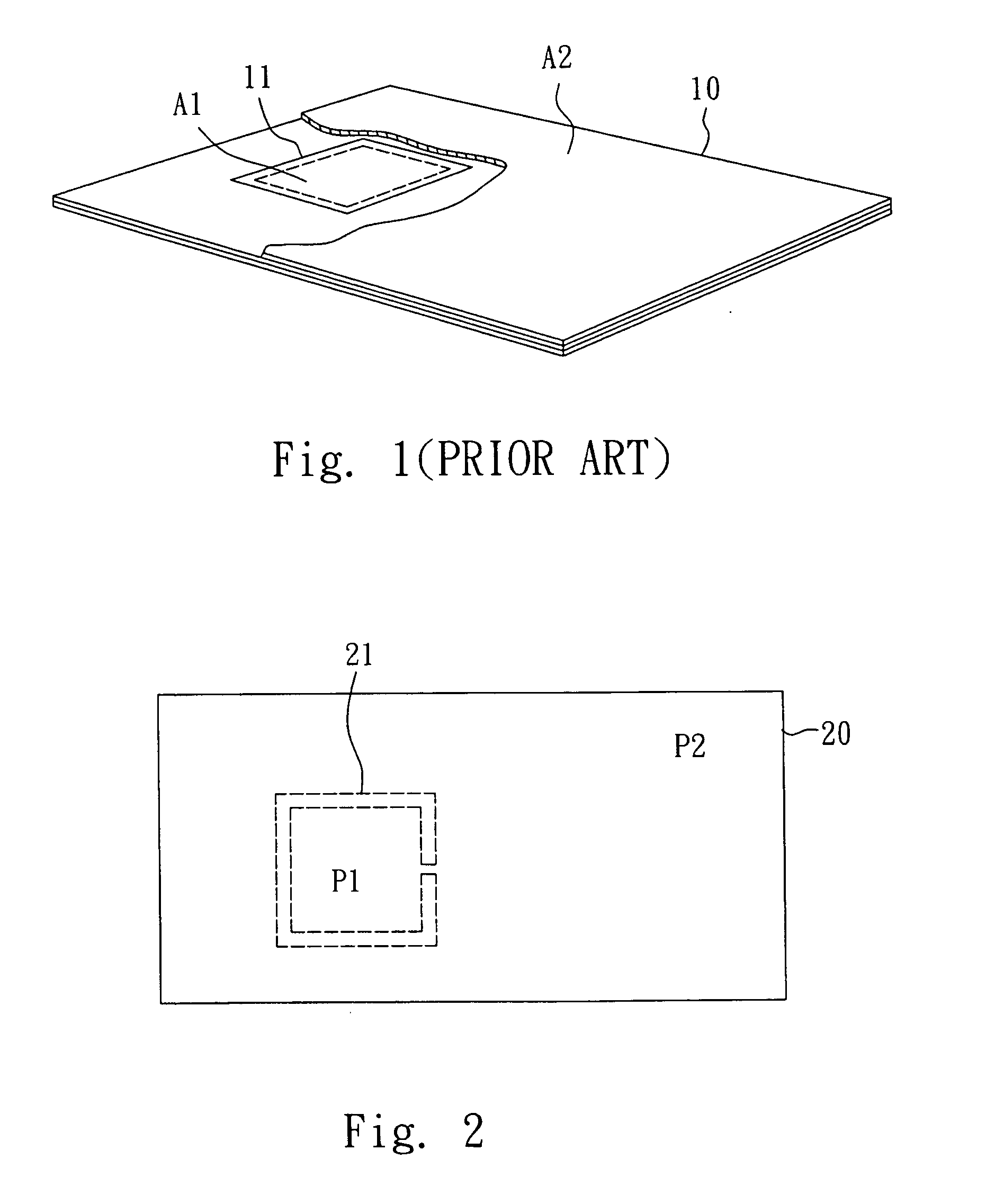
[0017] First, a printed circuit board (with dimensions of 74 mm×142 mm) without a capacitor of the present invention, and a printed circuit board 20 with at least one prese...


PUM


Abstract

The present invention relates to a printed circuit board with low noise. A voltage source layer and a ground layer of the printed circuit board are divided into an analog reason and a digital area respectively via an isolation line, and adapted to conduct voltage source signal and ground signal respectively. Because the isolation line is an open pattern and a capacitor adapts to position near the opening, the noise and the electro-magnetic parameter of the printed circuit board are reduced.

Description

BACKGROUND OF THE INVENTION [0001] 1. Field of the Invention [0002] The present invention relates to a printed circuit board and, more particularly, to a printed circuit board with low noise. [0003] 2. Description of the Related Art [0004] As shown in FIG. 1, a printed circuit board 10 is composed of at least three circuit boards; one layer is a voltage source (power) layer, and another layer is a ground layer, the surface of which (either the top face or the bottom face) is used as a layout for signal lines (as a signal layer). At least one electronic component is placed on the top or the bottom layer of the printed circuit board 10 and its signal pins, voltage source pins, and ground pins are separately connected to other electronic components, the voltage source layer and the ground layer on the surface of the printed circuit board 10. The electronic components can be categorized into analog electronic components and digital electronic components based on their signal characteris...

Claims


Application Information

Patent Timeline
Patent Type & Authority Applications(United States)
IPC IPC(8): H05K1/00H05K1/02H05K7/06
CPCH05K1/0225H05K2201/09663H05K2201/093H05K1/0231
Inventor CHAO, SHIH-CHIEHHUANG, CHIH-WENLIAO, CHUH-LIN
Owner TATUNG COMPANY
Why Eureka
Try Eureka