Light emitting element and light emitting device

a technology of light emitting device and light emitting element, which is applied in the direction of basic electric elements, semiconductor devices, electrical equipment, etc., can solve the problems of not obtaining the effect of snosub>2 /sub>film, the light emitting device will not offer a high brightness, and the next problem of conventional led elements, etc., to achieve the effect of improving the external radiation efficiency

Inactive Publication Date: 2005-05-05
TOYODA GOSEI CO LTD
View PDF6 Cites 171 Cited by
  • Summary
  • Abstract
  • Description
  • Claims
  • Application Information

AI Technical Summary

Benefits of technology

[0015] It is an object of the invention to provide a light emitting element and a light emitting device that are provided with an improved external radiation efficiency in light radiated from the semiconductor layer.
[0018] a diffusion layer that diffuses light emitted from the light emitting layer to increase the external radiation efficiency of the light emitting element.
[0021] a diffusion layer that has a refractive index equal to or greater than that of the light emitting layer and that diffuses light emitted from the light emitting layer to increase the external radiation efficiency of the light emitting element,
[0025] a light extraction portion that is disposed on the protection layer to coat the surface of the light emitting element and to enhance the external radiation efficiency of light emitted from the light emitting layer.
[0028] a light extraction portion that is disposed on the protection layer to coat the surface of the light emitting element and to enhance the external radiation efficiency of light emitted from the light emitting layer; and

Problems solved by technology

However, the conventional LED elements have the next problems.
However, if the thin film does not have a large value of m, such light entered to this specific direction from the interface only occupies a small part of all light emitted from the light emitting layer.
On the other hand, in the case of light subjected to total reflection when being entered at an angle greater than its critical angle to the SnO2 interface from the GaN-based compound semiconductor layer, the abovementioned effect of SnO2 film is not obtained because return light as interference light to this light is not generated at the interface of the SnO2 film and the epoxy resin.
Thus, most of light will be confined in the semiconductor layers and therefore the light emitting device will not offer a high brightness.

Method used


Image

  • Light emitting element and light emitting device
  • Light emitting element and light emitting device
  • Light emitting element and light emitting device

Examples


first embodiment

Effect of First Embodiment

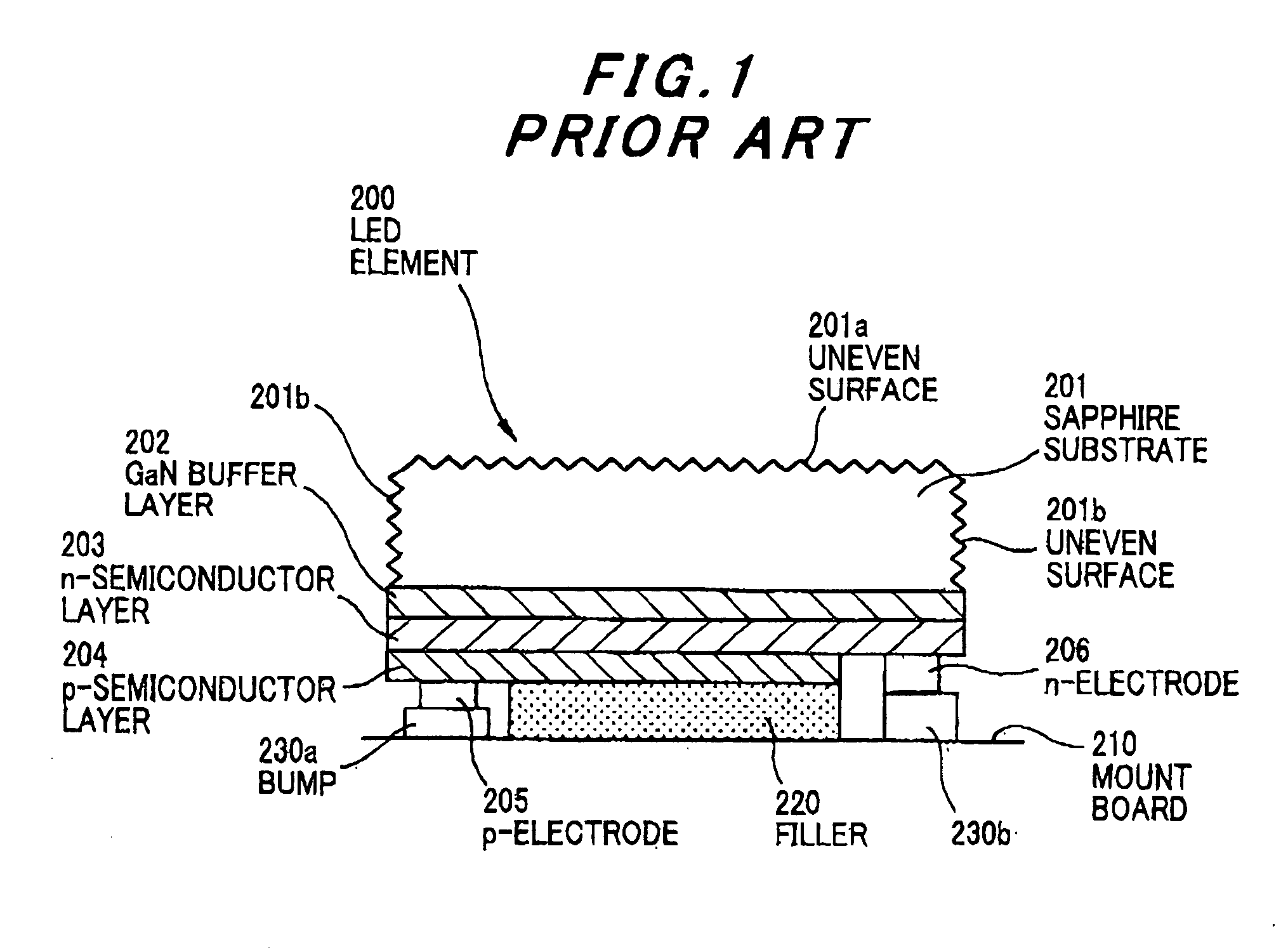
[0064] In the first embodiment, by providing the Al2O3 porous portion 20A on the light extraction surface of sapphire substrate 20, even part of light with an incident angle greater than the critical angle at the interface can be externally radiated while allowing the transmission (external radiation) of light with an incident angle smaller than the critical angle at the interface. Therefore, the light component to be attenuated due to the optical absorption in the LED element can be reduced and as a result the external radiation efficiency can be enhanced. In other words, even the light components in the range of θ2 to θ3 as shown in FIG. 3 can be externally radiated by using the Al2O3 porous portion 20A.

[0065] Further, even when the LED element 2 is sealed with epoxy resin, the light extraction property can be improved since the diffusion of light is also generated at the interface of air in the Al2O3 porous portion 20A and the surround.

Second Embodimen...

second embodiment

Effect of Second Embodiment

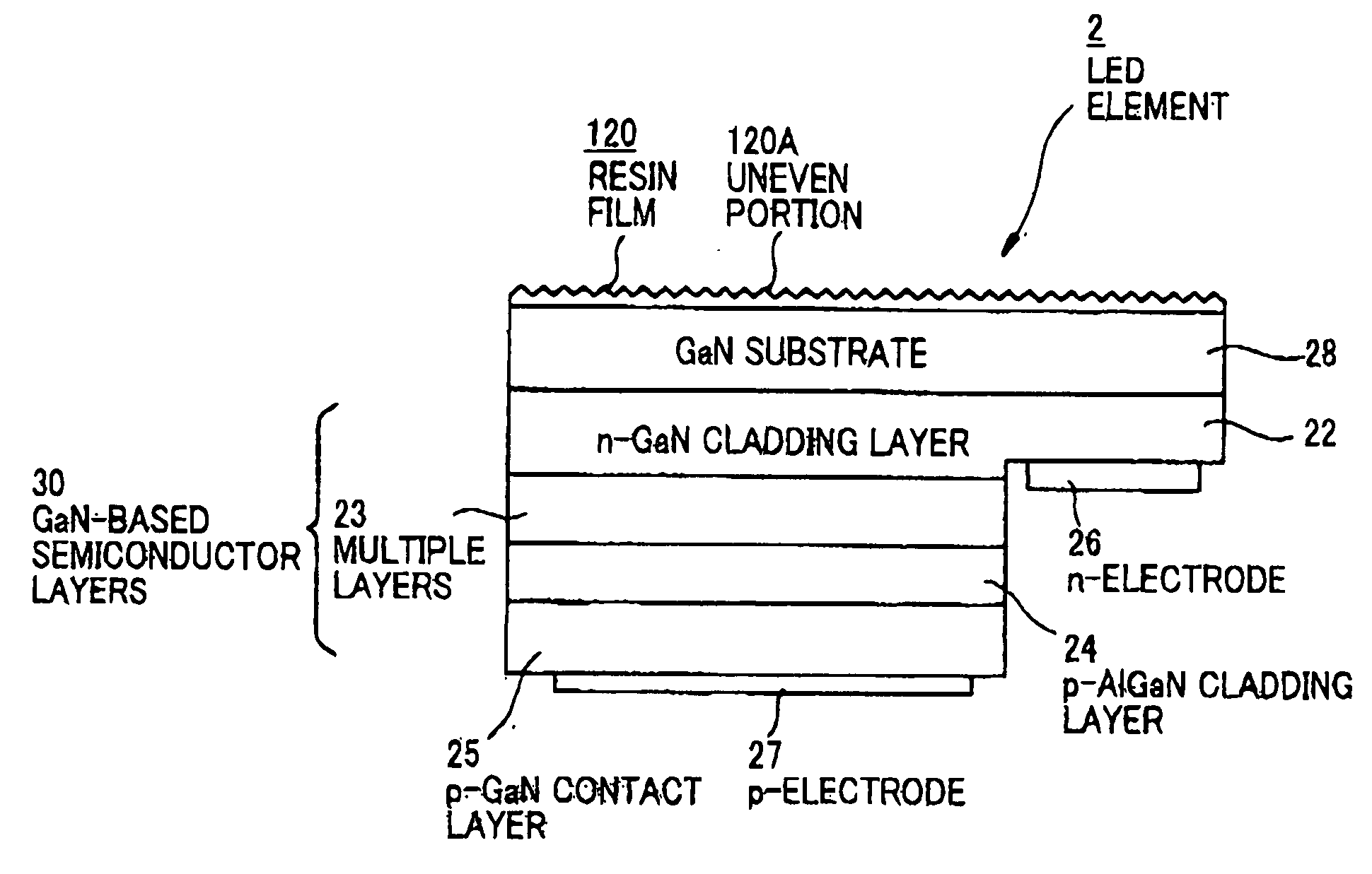
[0071] In the second embodiment, by using the GaN substrate 28, light generated from the multiple layers 23 is not subjected to reflection at the interface of the nitride-based semiconductor layers 30 and the GaN substrate 28.

[0072] Further, by providing the TiO2 porous portion 28A with a refractive index greater than that of the GaN substrate 28 on the light extraction face of GaN substrate 28, the reflection at the interface of the GaN substrate 28 and the TiO2 porous portion 28A can be reduced and the entering of light into the TiO2 porous portion 28A can be more increased. As a result, the external radiation efficiency can be enhanced.

[0073] Further, since the TiO2 porous portion 28A is included in the apparent size of LED element 2 as a light emitting body, the light emitting element can offer high brightness as compared to the conventional light emitting element with the same size. Namely, the LED element 2 with the TiO2 porous portion 28A can have...

third embodiment

[0075] [Composition of LED Element 2]

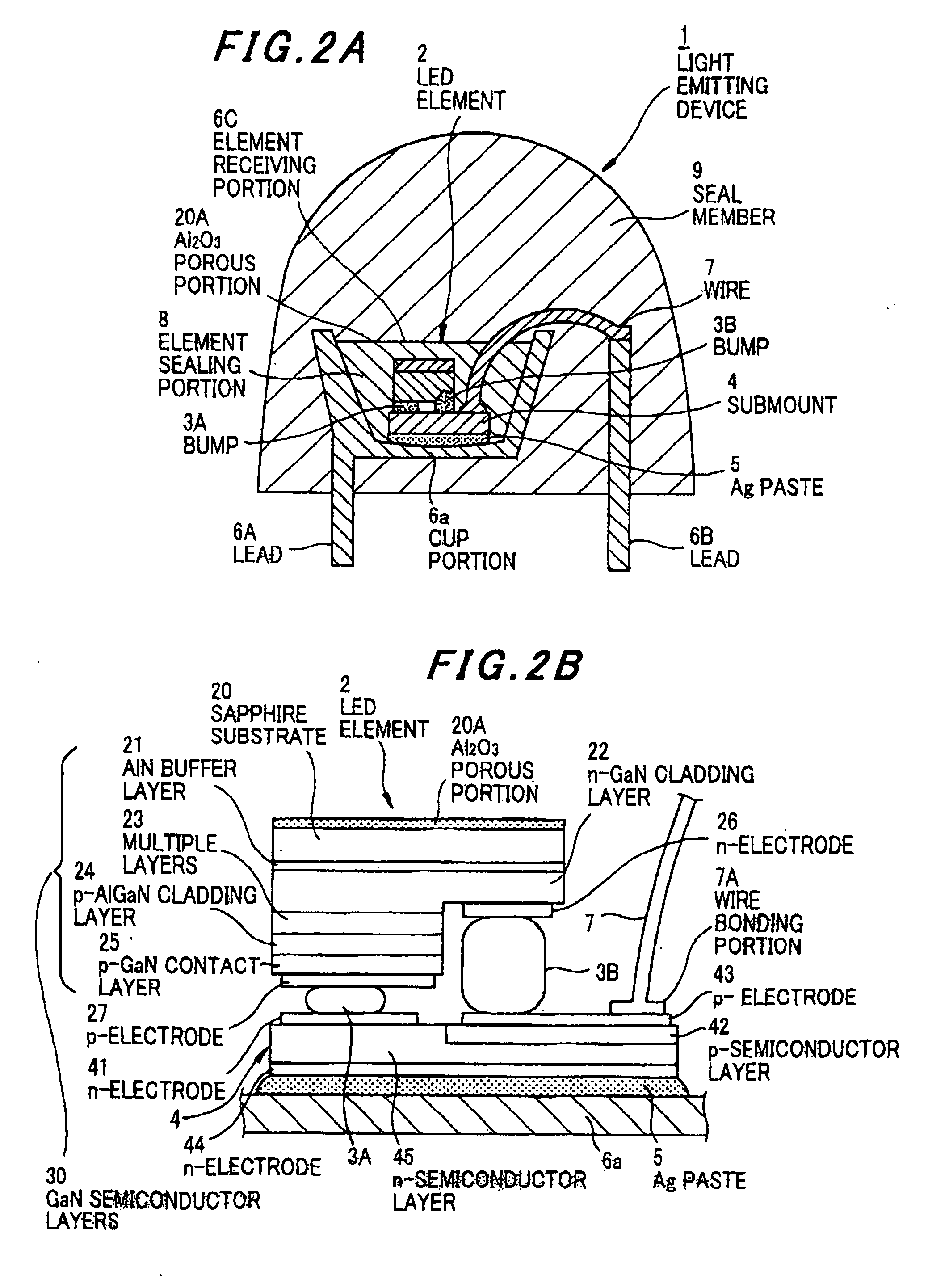
[0076]FIG. 5 is an enlarged cross sectional view showing part of an LED element in the third preferred embodiment according to the invention.

[0077] The LED element 2 of the third embodiment is different from that of the second embodiment in that a TiO2 portion 28B composed of transparent TiO2 particles 28a and TiO2 coating film 28b covering the TiO2 particles 28a is formed on the GaN substrate 28 instead of the TiO2 porous portion 28A. Thus, the TiO2 particle 28a as a transparent particle allows the TiO2 coating film 28b, which is transparent to emission wavelength, to have an uneven surface, whereby light entering into the TiO2 coating film 28b is diffused.

[0078] The TiO2 portion 28B is formed by sol-gel method using Ti alkoxide containing the powered TiO2 particles 28a on the light extraction face side of GaN substrate 28, where the TiO2 portion 28B is formed thin film after conducting the thermal decomposition of Ti alkoxide. It is required ...


PUM


Abstract

A light emitting element has: a light emitting layer of semiconductor; and a diffusion layer that has a refractive index equal to or greater than that of the light emitting layer and that diffuses light emitted from the light emitting layer to increase the external radiation efficiency of the light emitting element. The light emitting layer has a refractive index equal to or greater than that of any layers formed between the light emitting layer and the diffusion layer.

Description

[0001] The present application is based on Japanese patent application Nos. 2003-373273, 2003-401120 and 2004-109431, the entire contents of which are incorporated herein by reference. BACKGROUND OF THE INVENTION [0002] 1. Field of the Invention [0003] This invention relates to a light emitting element and a light emitting device using the same, and particularly relates to a light emitting element and a light emitting device that are provided with an improved external radiation efficiency in light radiated from the semiconductor layer. [0004] 2. Description of the Related Art [0005] Conventionally, light emitting devices are known that an LED (light emitting diode) element is mounted on a substrate with a lead frame or a wiring pattern formed thereon. For such light emitting devices, it is important to increase the external radiation efficiency by reducing light confined in the LED element to offer high brightness and output. [0006] The LED element used for the light emitting device...

Claims


Application Information

Patent Timeline
Patent Type & Authority Applications(United States)
IPC IPC(8): H01L29/22H01L33/22H01L33/32H01L33/36H01L33/44H01L33/50H01L33/56H01L33/60H01L33/62
CPCH01L33/44H01L2933/0091H01L2224/45144H01L2224/73265H01L2224/48247H01L2224/16145H01L2224/32245H01L2224/48091H01L2224/48465H01L2924/00014H01L2924/00H01L2224/05573H01L2224/05568H01L2924/181H01L2224/48257H01L2224/49107H01L2224/06102H01L2224/1703H01L2924/00012
Inventor SUEHIRO, YOSHINOBUNAKAJO, NAOKI
Owner TOYODA GOSEI CO LTD
Why Eureka
Try Eureka