
Connection pin

Inactive Publication Date: 2005-05-05
NIHON DENSHIZAIRYO
View PDF15 Cites 16 Cited by
  • Summary
  • Abstract
  • Description
  • Claims
  • Application Information

AI Technical Summary

Benefits of technology

[0009] It is an object of the present invention to provide a connection pin which can be easily detached one-by-one and provides stable electrical connection even after repetitive use, in a probe card for testing a semiconductor device.
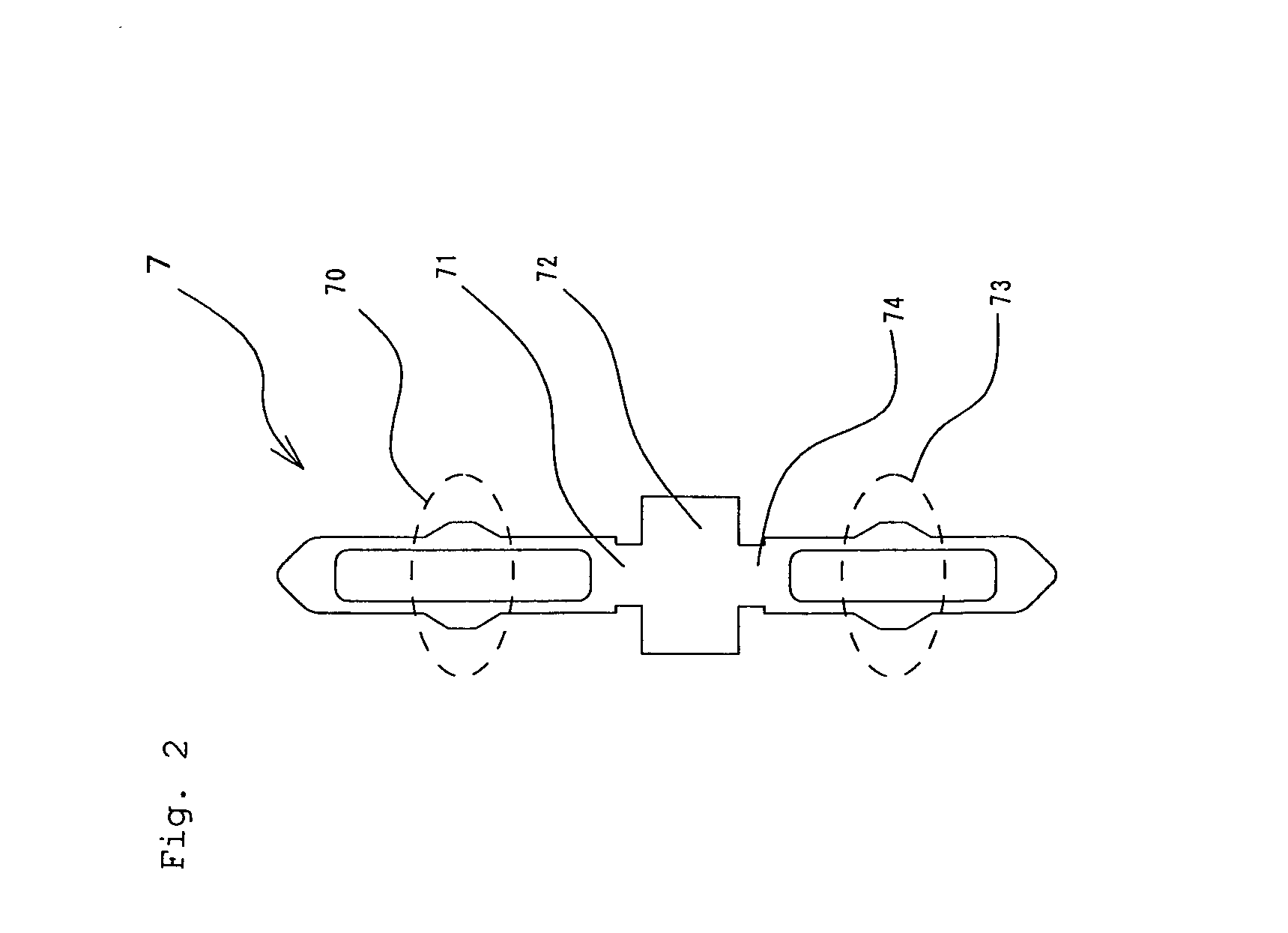
[0012] Thus, according to the present invention, the connection pin detachably provides electrical connection between the first and second substrates having the through-holes, and comprises the first contact part which comes in contact with the through-hole provided in the first substrate, the first support part which supports the first contact part, the stopper which abuts on the surfaces of the first and second substrates, the second contact part which comes in contact with the through-hole provided in the second substrate, and the second support part which supports the second contact part, in which the first and second contact parts have spring properties and elastically come into contact with the side walls of the through-holes provided in the first and second substrates. As a result, it is easily detachable one-by-one and provides stable electrical connection even after repetitive use.
[0013] In addition, according to the connection pin of the present invention, since there are provided the plurality of first and / or second contact parts, its contact area is increased and further stable electrical connection is provided.

Problems solved by technology

The lateral type of probe card has an aspect which is not suitable for measuring many chips at the same time, which is required under the circumstances in which large-scale integration of the LSI chip is implemented and a tester is multiplexed, so that it is less used nowadays.
However, according to this type of connection pin, when a substrate constitution of the probe card is changed according to the kind of the semiconductor device to be tested, since the connection pin cannot be removed from the second substrate, the constitution which can correspond to the semiconductor device to be tested is limited.
Furthermore, when a connection pin is bent or broken, since it is not possible only that connection pin is removed, the second substrate has to be entirely exchanged in that case.
Still further, since the plurality of connection pins are completely fixed to the second substrate, if each connection pin is slightly shifted in position, it is difficult for the connection pin to be inserted.

Method used


Image

  • Connection pin
  • Connection pin
  • Connection pin

Examples


Embodiment Construction

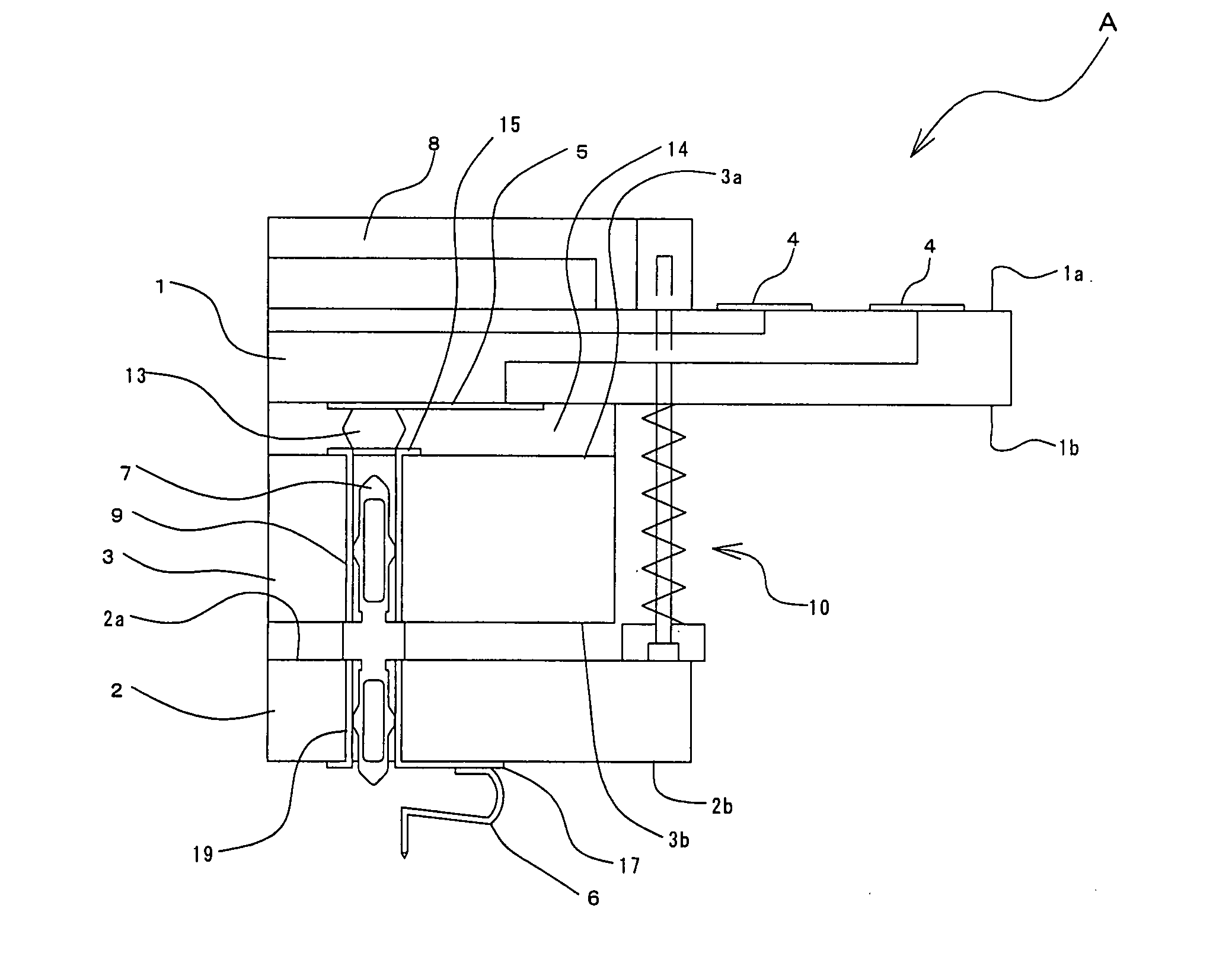
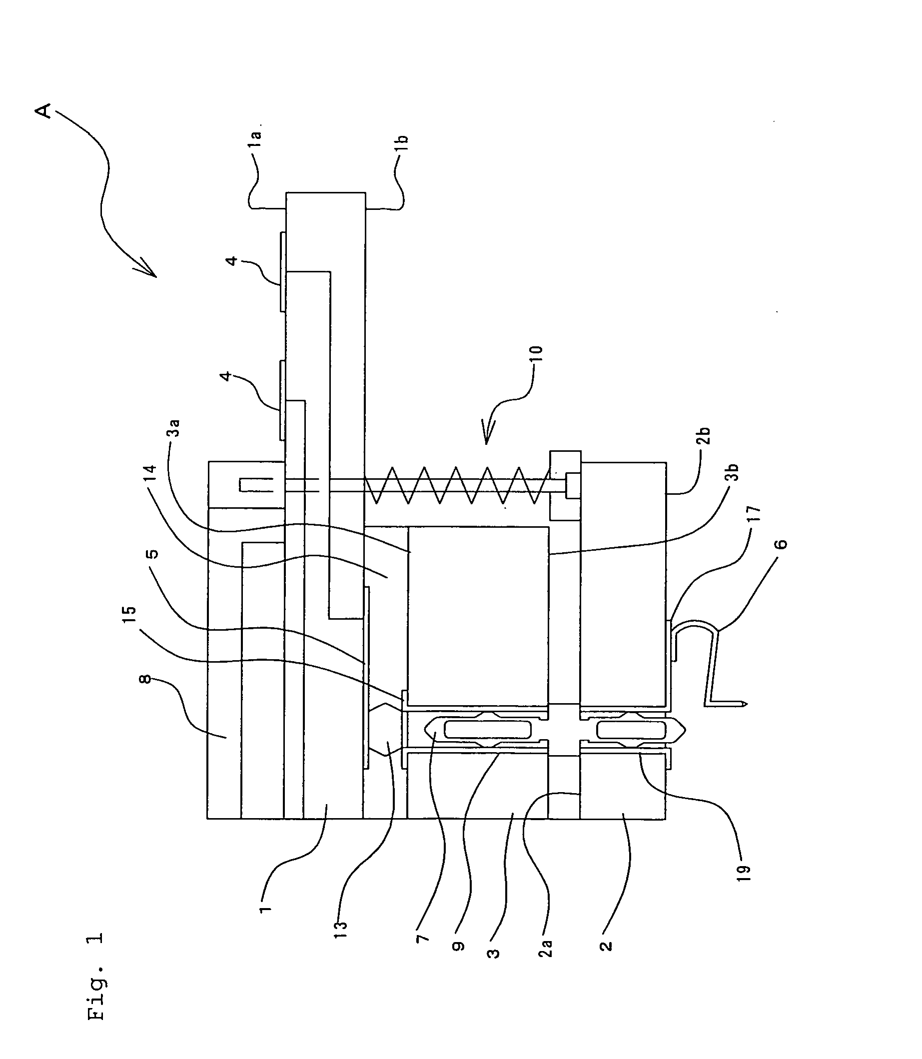
[0019] A probe card A, as apart of it is shown in FIG. 1, comprises a main substrate 1 having first connection electrodes 4 which come in contact with a measuring device for testing such as a tester (not shown), a sub-substrate 3 having a plurality of through-holes 9 electrically connected to the first connection electrode 4, a space transformer 2 having a plurality of through-holes 19 electrically connecting a one main surface 2a to the other main surface 2b and comprising a plurality of contactors 6 on the other main surface 2b, which come into contact with a semiconductor device (not shown) which is a tested object such as an IC chip or the like, a connection pin 7 which is detachably inserted to the through-hole 9 in the sub-substrate 3 and the through-hole 19 in the space transformer 2, and a holding jig 10 which detachably mounts the space transformer 2 on the main substrate 1.

[0020] As shown in FIG. 1, the main substrate 1 comprises the plurality of first connection electrod...


PUM


Abstract

It is an object of the present invention to provide a connection pin for a probe card which measures electrical characteristics of a semiconductor device such as a LSI ship. The connection pin for the probe card which tests the semiconductor device has a U-shaped or V-shaped spring part manufactured by etching or pressing of metal.

Description

BACKGROUND OF THE INVENTION [0001] 1. Field of the Invention [0002] The present invention relates to a connection pin for electrically connecting a plurality of substrates which constitute a probe card for measuring electrical characteristics of a semiconductor device such as an LSI chip. [0003] 2. Description of the Background Art [0004] There are a lateral type called cantilever type and a vertical type called perpendicular type in a probe card which measures electrical characteristics of a semiconductor device such as a LSI chip. The lateral type of probe card has an aspect which is not suitable for measuring many chips at the same time, which is required under the circumstances in which large-scale integration of the LSI chip is implemented and a tester is multiplexed, so that it is less used nowadays. Meanwhile, since the vertical type of probe card can use many probes and provides a high degree of freedom for a probe arrangement and it is suitable for measuring many chips at t...

Claims


Application Information

Patent Timeline
IPC IPC(8): G01R1/04G01R1/073G01R1/067G01R31/02G01R31/28H01R12/58
CPCH01R12/58G01R1/0416H01R12/585
Inventor MORI, CHIKAOMINAKASHIMA, MASANARI
Owner NIHON DENSHIZAIRYO
Learn More