

Liquid crystal display device and method of manufacturing the same
a liquid crystal display and liquid crystal technology, applied in non-linear optics, instruments, optics, etc., can solve the problems of reducing productivity, difficult to precisely determine the amount of liquid crystal applied on the substrate, contamination of liquid crystal b>5/b>, etc., to improve picture quality characteristics and uniform cell gaps
- Summary
- Abstract
- Description
- Claims
- Application Information
AI Technical Summary
Benefits of technology
Problems solved by technology
Method used
Image

Examples
first embodiment
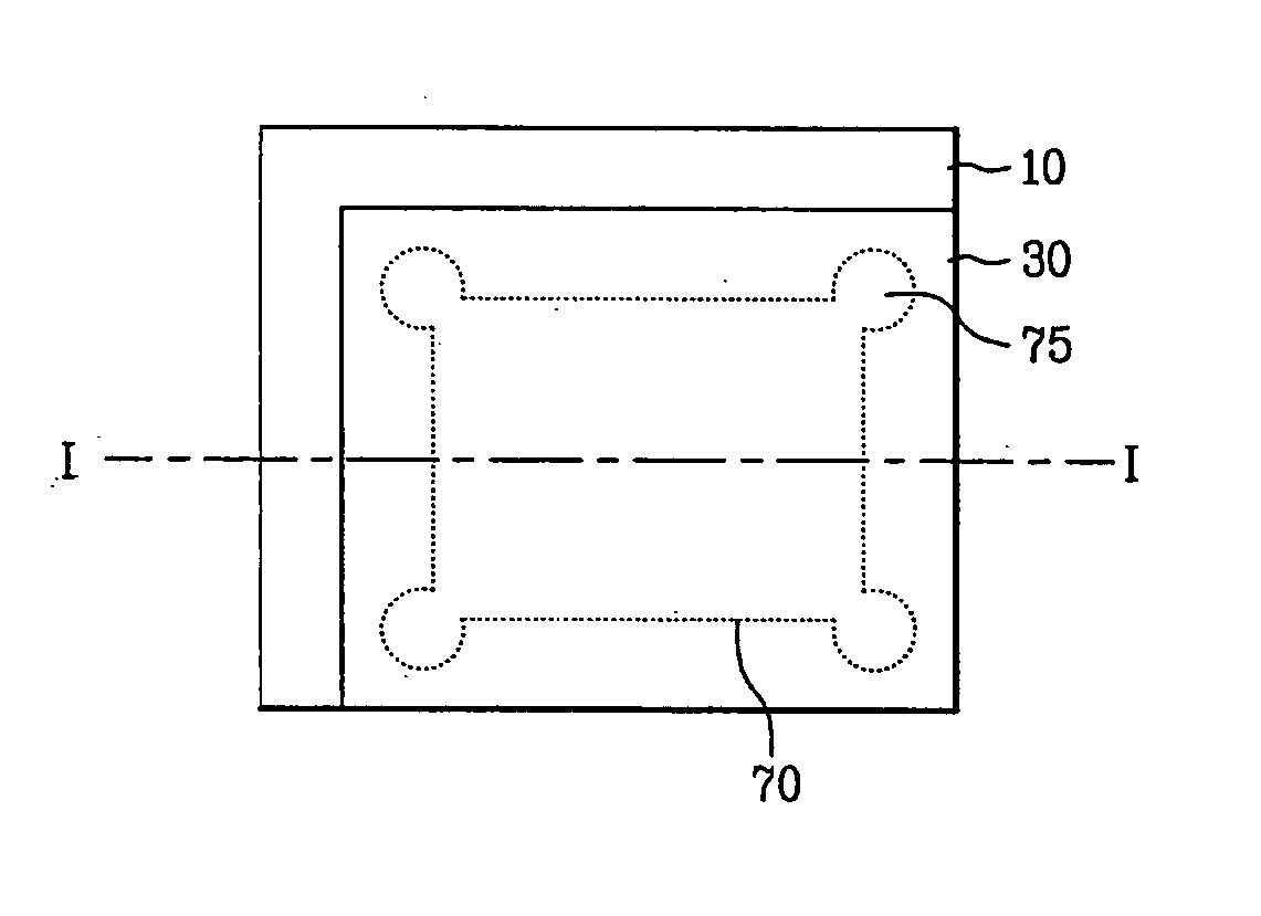
[0043]FIG. 3A is a plan view of an LCD device according to the present invention, and FIG. 3B is a sectional view taken along line I-I of FIG. 3A.
[0044] As shown in FIGS. 3A and 3B, an LCD device according to the first embodiment of the present invention includes a lower substrate 10, an upper substrate 30, a sealant 70 that is at least partially curable by ultraviolet (UV) light formed between the lower and upper substrates 10 and 30, and a liquid crystal layer 50 formed within a volume formed by the UV sealant 70 between the lower and upper substrates 10 and 30.
[0045] The UV sealant 70 is patterned to form a part 75 for controlling a liquid crystal flow at four corner regions. The part 75 is formed to receive excess liquid crystal from an active region of the LCD device, such as a cavity, reservoir or well. Therefore, if the liquid crystal is applied excessively, i.e., overfilled, the excess liquid crystal enters into the part 75 away from an active region.
[0046] Also, even if t...
second embodiment
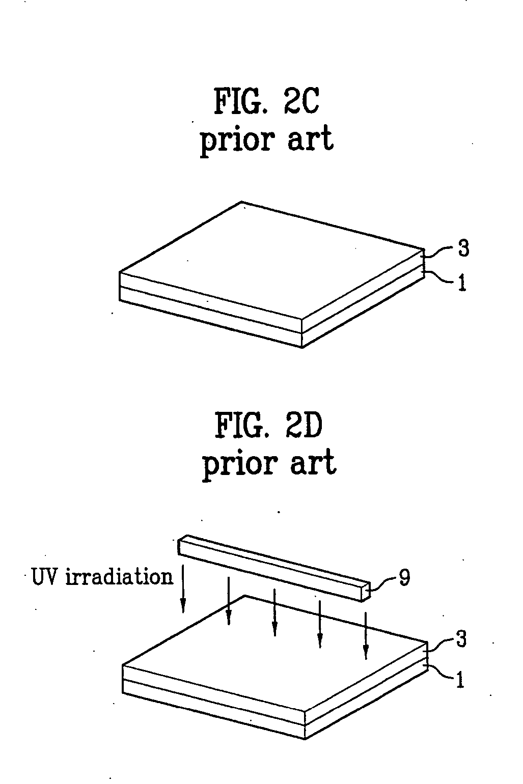
[0052]FIGS. 4A to 4D are perspective views illustrating a method of manufacturing an LCD device according to the present invention.
[0053] Although the drawings illustrate only one unit cell, a plurality of unit cells may be formed depending upon the size of the substrate.
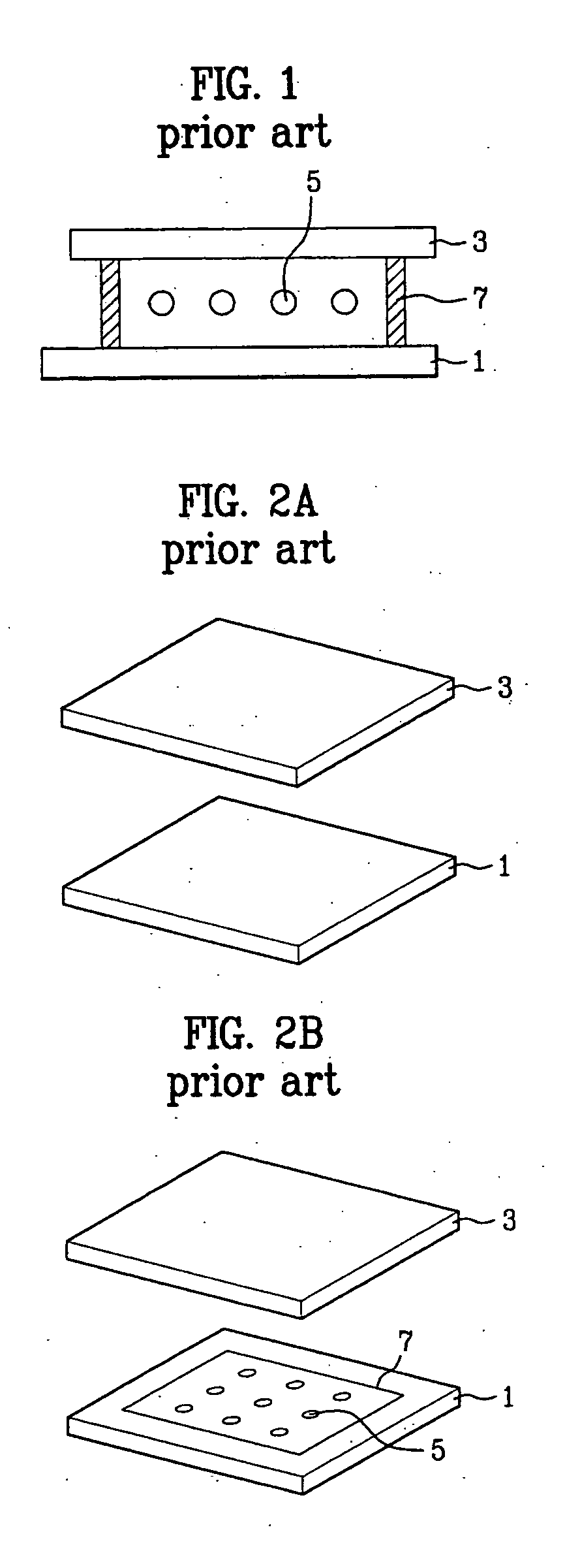
[0054] Referring to FIG. 4A, a lower substrate 10 and an upper substrate 30 are prepared. A plurality of gate and data lines (not shown) are formed on the lower substrate 10. The gate lines cross the data lines to define a pixel region. A thin film transistor having a gate electrode, a gate insulating layer, a semiconductor layer, an ohmic contact layer, source / drain electrodes, and a protection layer is formed at each crossing point of the gate lines and the data lines. A pixel electrode connected with the thin film transistor is formed in the pixel region.
[0055] An alignment film (not shown) is formed on the pixel electrode to initially align the liquid crystal. The alignment film may be formed of polyamide or p...
PUM
 Abstract
Description
Claims
Application Information