Narrow bezel display panel and preparation method thereof, and narrow bezel display device

a display panel and narrow bezel technology, applied in the field of display technology, can solve the problems of high manufacturing cost, difficult reduction of the bezel relative difficulty in design and process, and achieve the effect of reducing the width of the display panel, reducing the gap of the plane region, and high light transmittan

Inactive Publication Date: 2021-04-01
SHENZHEN CHINA STAR OPTOELECTRONICS TECH CO LTD
View PDF0 Cites 1 Cited by
  • Summary
  • Abstract
  • Description
  • Claims
  • Application Information

AI Technical Summary

Benefits of technology

[0009]Advantages of the present disclosure are that the present disclosure can realize transformation between flexibility and rigidity of the base substrate by selecting a flexible photo-curable macromolecule resin material having high light transmittance and by a selective exposure process. The bending region of the base substrate is flexible, and can be bent to hide on the back surface of the base substrate, which greatly reduces a width of the display panel to realize a narrow bezel of the display panel; the plane region of the base substrate is rigid, and can remain a stable cell gap when be bent, thereby preventing the cell gap on the plane region from changing, causing uneven display phenomenon (Mura) when the bending region is bent, thereby ensuring the cell gap of the plane region to be uniform. The present disclosure can realize the ultra-narrow bezel design requirement while can ensure uniformity of the in-plane cell gap thickness, and the process is compatible with the existing process, and has advantages of simple manufacturing and low cost.

Problems solved by technology

Therefore, depending on the size of the peripheral circuits, the bezels of the panels are difficult to reduce.
However, the two technical designs and processes are relative difficult and the manufacturing cost is high.

Method used


Image

  • Narrow bezel display panel and preparation method thereof, and narrow bezel display device
  • Narrow bezel display panel and preparation method thereof, and narrow bezel display device
  • Narrow bezel display panel and preparation method thereof, and narrow bezel display device

Examples


Embodiment Construction

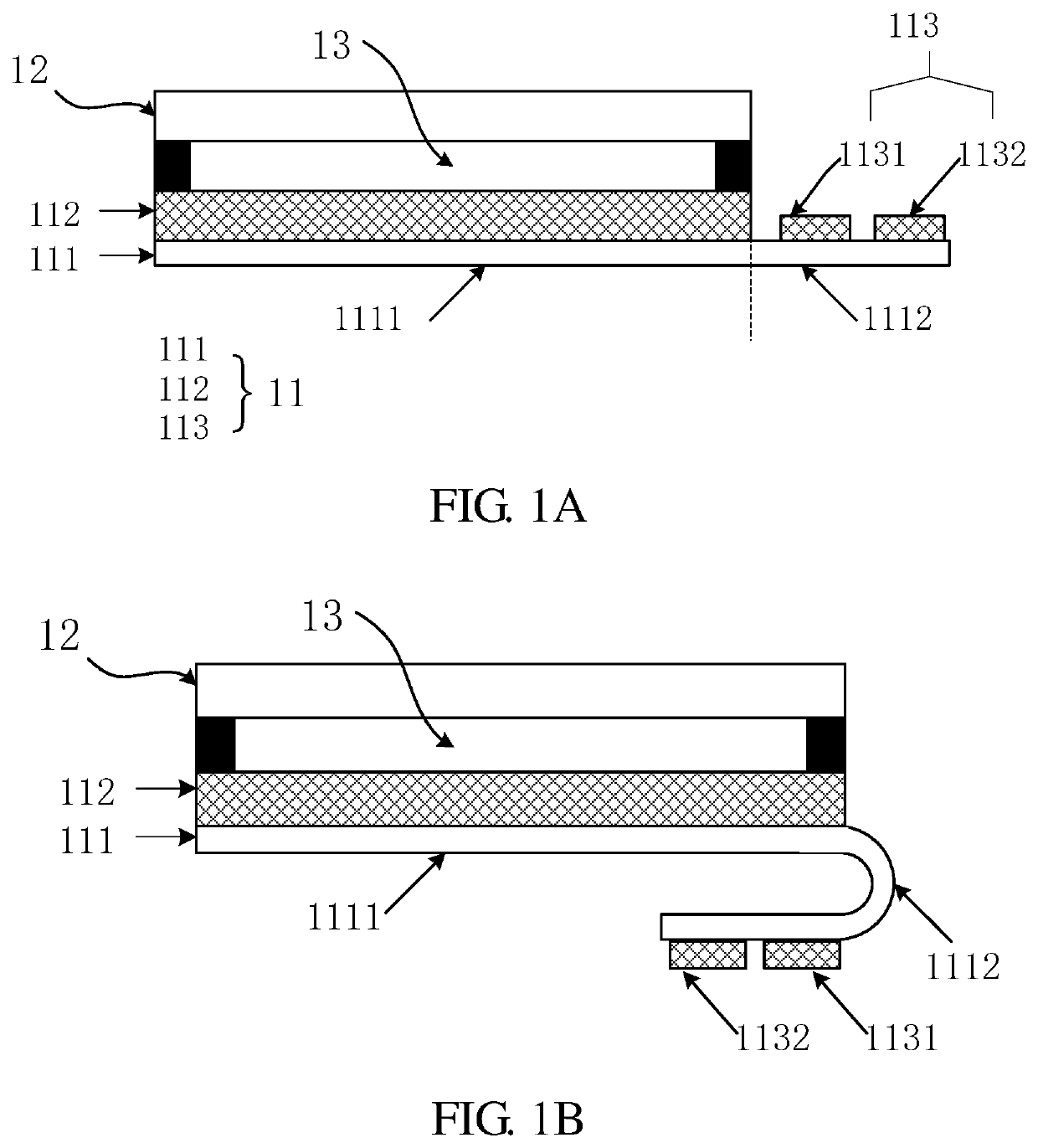
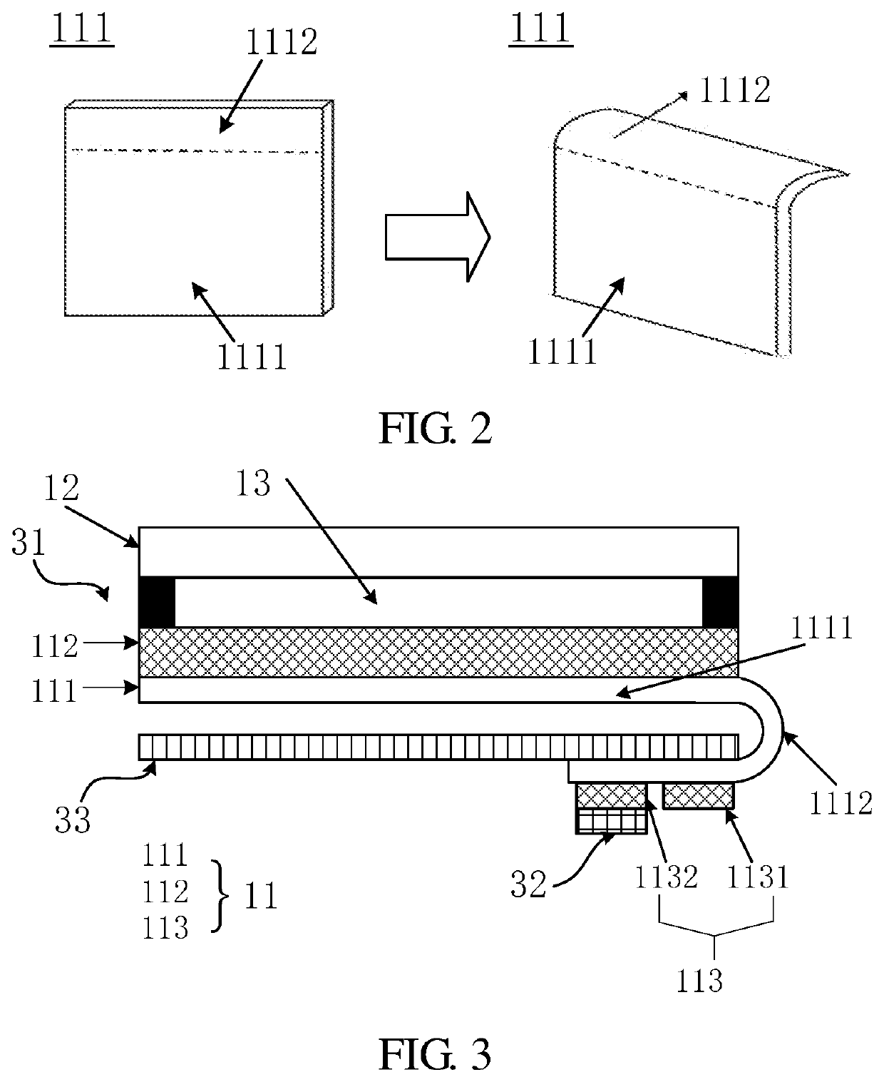
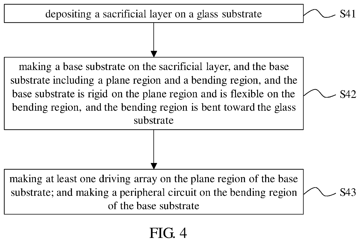
[0017]The embodiments of the present disclosure are described in detail hereinafter. Examples of the described embodiments are given in the accompanying drawings, wherein the identical or similar reference numerals constantly denote the identical or similar elements or elements having the identical or similar functions. The specific embodiments described with reference to the accompanying drawings are all exemplary and are intended to illustrate and interpret the present disclosure, which shall not be construed as causing limitations to the present disclosure.

[0018]In the present disclosure, unless expressly specified or limited otherwise, a first feature is “on” or “beneath” a second feature may include that the first feature directly contacts the second feature and may also include that the first feature does not directly contact the second feature. Furthermore, a first feature “on,”“above,” or “on top of” a second feature may include an embodiment in which the first feature is ri...


PUM

PropertyMeasurementUnit
thicknessaaaaaaaaaa
visible light transmittanceaaaaaaaaaa
transmittanceaaaaaaaaaa

Abstract

A narrow bezel display panel and preparation method thereof, and a narrow bezel display device, which can realize transformation between flexibility and rigidity of the base substrate by selecting a flexible photo-curable macromolecule resin material having high light transmittance and by a selective exposure process. A bending region of a base substrate is flexible, and can be bent to hide on a back surface of a base substrate to realize a narrow bezel of the panel; a plane region of the base substrate is rigid, and can remain a stable cell gap during bending.

Description

FIELD OF INVENTION[0001]The present disclosure relates to field of display technology, and particularly relates to a narrow bezel display panel and preparation method, and narrow bezel display device thereof.BACKGROUND OF INVENTION[0002]Liquid crystal displays (LCDs) have advantages, such as energy conservation, lightness and thinness, and exquisite graphics, etc., and have been widely used in the field of display technology. Liquid crystal displays are generally composed of an upper substrate, a bottom substrate, and a liquid crystal layer (LCL) disposed between the two substrates. The upper substrate and the bottom substrate are respectively fabricated. A thin film transistor array (TFT) is disposed on the bottom substrate, and a color filter is disposed on the upper substrate. A liquid crystal cell is formed after the upper substrate and bottom substrate are assembled to each other, and periphery of the liquid crystal cell is sealed using a frame glue. The wider the bezel, the pe...

Claims


Application Information

Patent Timeline
Patent Type & Authority Applications(United States)
IPC IPC(8): G02F1/1345G02F1/1333G02F1/1335
CPCG02F1/13452G02F1/133514G02F1/133305G03F7/0757G03F7/0387Y02E10/549Y02P70/50H10K77/111G02F1/133368G03F7/004G06F1/1652G09G2380/02H10K71/00
Inventor ZHOU, KAIFENG
Owner SHENZHEN CHINA STAR OPTOELECTRONICS TECH CO LTD
Why Eureka
Try Eureka