Liquid crystal display device
- Summary
- Abstract
- Description
- Claims
- Application Information
AI Technical Summary
Benefits of technology
Problems solved by technology
Method used
Image
Examples
first exemplary embodiment
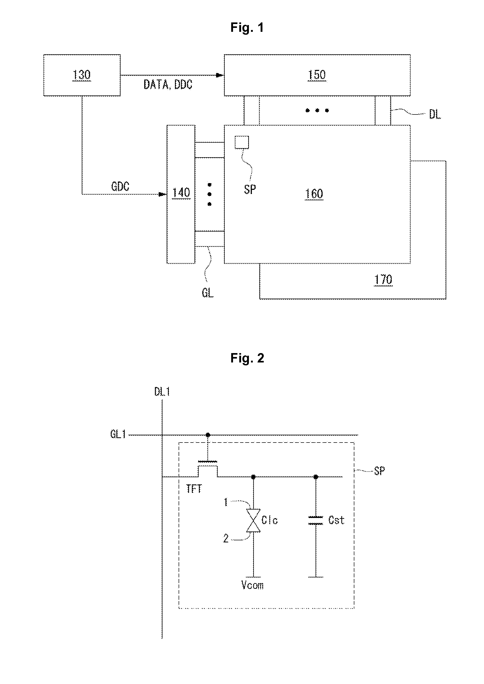
[0030]FIG. 1 is a block diagram schematically illustrating a liquid crystal display (LCD) device according to a first exemplary embodiment of the present invention. FIG. 2 is a circuit diagram schematically illustrating a sub-pixel shown in FIG. 1.
[0031]As illustrated in FIGS. 1 and 2, the LCD device includes a timing controller 130, a gate driver 140, a data driver 150, a liquid crystal panel 160, and a backlight unit 170.
[0032]The timing controller 130 receives a vertical synchronization signal Vsync, a horizontal synchronization signal, a data enable signal, a clock signal, and a data signal DATA from the outside. The timing controller 130 controls operation timing of the data driver 150 and the gate driver 140 by using timing signals such as the vertical synchronization signal, the horizontal synchronization signal, the data enable signal, and the clock signal.
[0033]The timing controller 130 may count the data enable signal during one horizontal period to determine a frame perio...
second exemplary embodiment
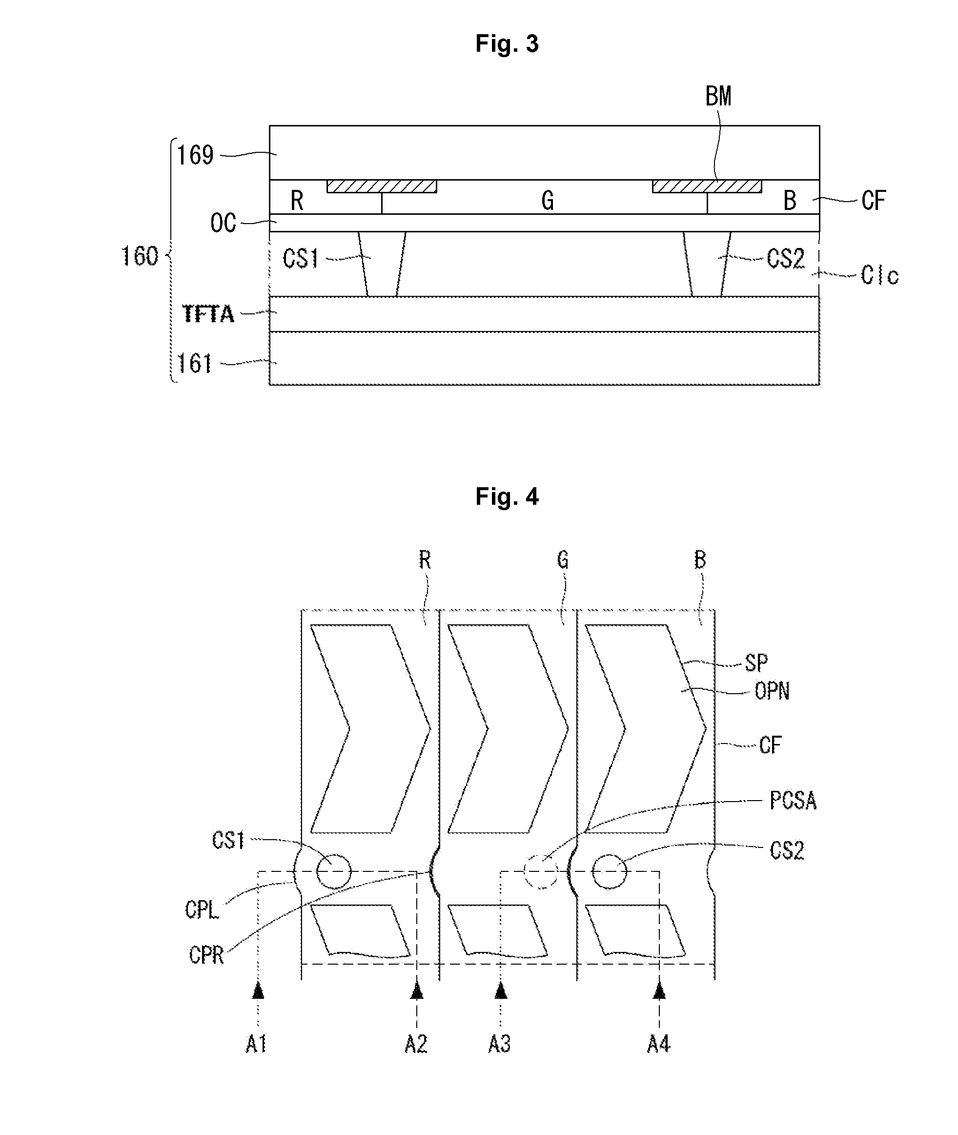
[0065]FIG. 10 is an exemplified cross-sectional view illustrating a liquid crystal panel according to a second exemplary embodiment of the present invention. FIG. 11 is an exemplified top-plan view illustrating an internal surface of an upper substrate of the liquid crystal panel of FIG. 10. FIG. 12 is a view illustrating color filter and column spacer portions. FIG. 13 is a view specifically illustrating a structure of the color filter. FIG. 14 is a view illustrating a structural effect according to the second exemplary embodiment of the present invention.
[0066]As illustrated in FIGS. 10 and 11, a thin film transistor array TFTA is formed on a lower substrate 161. The thin film transistor array TFTA includes the thin film transistor TFT and the storage capacitor Cst shown in FIG. 2. The thin film transistor array TFTA may be formed to have various structures according to a shape of the thin film transistor TFT, the storage capacitor Cst, a pixel electrode, and a common electrode (t...
PUM
 Abstract
Description
Claims
Application Information


