Substrate, liquid crystal display device, and method of manufacturing the same

a liquid crystal display device and substrate technology, applied in non-linear optics, instruments, optics, etc., can solve the problems of abnormal arrangement of liquid crystal molecules near the ball spacer, deterioration of display quality of liquid crystal display devices, and abnormal cell gap, so as to improve display quality and uniform cell gap

Active Publication Date: 2005-05-12
SAMSUNG DISPLAY CO LTD
View PDF4 Cites 52 Cited by
  • Summary
  • Abstract
  • Description
  • Claims
  • Application Information

AI Technical Summary

Benefits of technology

[0035] The liquid crystal display apparatus maintains a uniform cell gap, even though a compressive stress of a center portion of the liquid crystal display apparatus is different from a compressive stress of an edge portion of the liquid crystal display apparatus. Therefore, display quality is enhanced.
[0036] According to the method o

Problems solved by technology

When a thickness of the liquid crystal layer (or a cell gap between the thin film transistor substrate and the color filter substrate) is non-uniform, a display quality of the liquid crystal display device is deteriorated.
Firstly, the ball spacer is deformable and scattered irregularly, so that the cell gap is not uniform.
Secondly, a liquid crystal molecule near the ball spacer is abnormally arranged to lower a luminance.
Thirdly, reducing the diameter of the ball spacer is very hard, so that making a short cell gap is also very hard.
Fourthly, the ball spacer may be disposed on a pixel to deteriorate a display quality.
Thus, a rigid spacer formed at the center ‘B’ is compressed more than a rigid spacer formed at the edges ‘A’ and ‘C’, so that the rigid spacer formed at the center ‘B’ or the center

Method used


Image

  • Substrate, liquid crystal display device, and method of manufacturing the same
  • Substrate, liquid crystal display device, and method of manufacturing the same
  • Substrate, liquid crystal display device, and method of manufacturing the same

Examples


embodiment 1

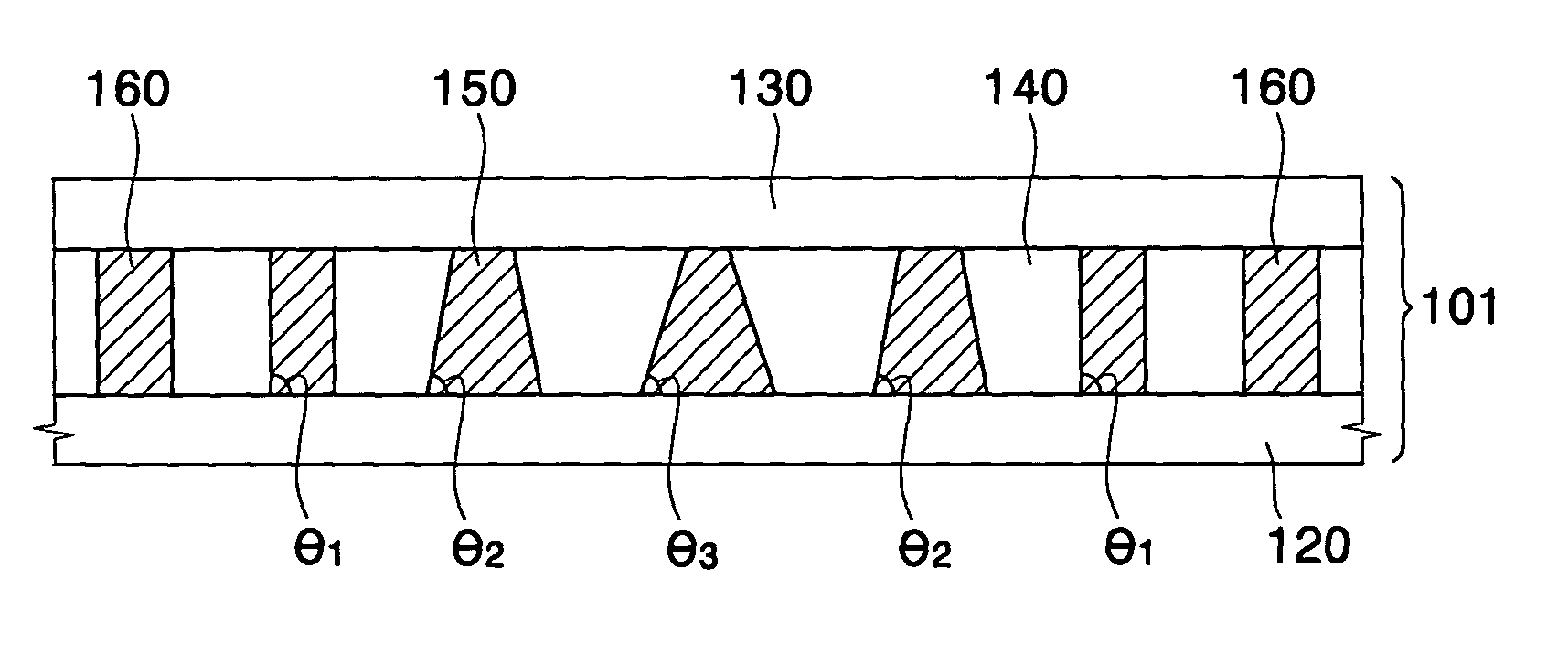
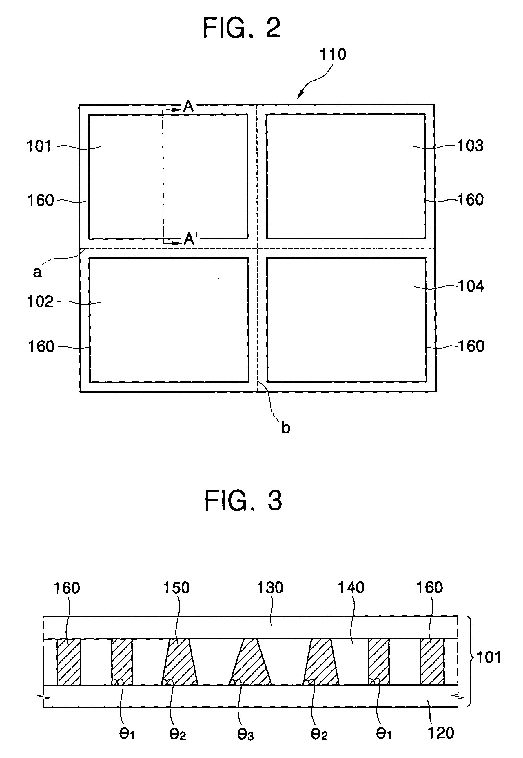
[0081]FIG. 2 is a schematic plan view showing a mother substrate of liquid crystal display panel according to a first exemplary embodiment, and FIG. 3 is a cross-sectional view taken along a line A-A′ of FIG. 2.

[0082] Referring to FIGS. 2 and 3, a mother substrate 110 of a liquid crystal display panel includes a plurality of liquid crystal display panels 101, 102, 103 and 104.

[0083] The mother substrate 110 includes two substrates 120 and 130, and a liquid crystal layer interposed between the two substrates 120 and 130. Each of the liquid crystal display panels 101, 102, 103 and 104 includes a display region.

[0084] A plurality of spacers 150 is formed between the two substrates 110 and 120. The spacers 150 maintain a cell gap that is a distance between the two substrates 110 and 120.

[0085] The liquid crystal layer 140 is confined within a space defined by the two substrates 110 and 120, and a fence 160.

[0086] As shown in FIG. 3, the spaces 150 have different tapered angles θ1, ...

embodiment 2

[0091]FIG. 4 is a cross-sectional view showing a liquid crystal display apparatus according to a second exemplary embodiment.

[0092] The liquid crystal display apparatus of the present embodiment is similar to the liquid crystal display apparatus of Embodiment except that a shape of the spaces is different from that of Embodiment 1. Thus, in FIG. 4, the same reference numbers will be used to refer to the same or like parts as those shown in FIG. 3.

[0093] Referring to FIGS. 2 and 4, spacers 170 support the two substrates 120 and 130. A diameter of the spacers 170 becomes smaller in a direction from the center to the edge, so that a compression ratio becomes larger in the direction.

[0094] In other word, an area of a contact face between the spacers 170 and the two substrates 120 and 130 becomes smaller in a direction from the center to the edge.

[0095] Thus, the cell gap of the center is substantially equal to the cell gap of the edge, even though the compression at the center is la...

embodiment 3

[0106]FIG. 5 is a cross-sectional view showing a liquid crystal display apparatus according to a third exemplary embodiment.

[0107] Referring to FIG. 5, each of spacers 180 has a same shape. However, a compression ratio of the spacers 180 is different from each other.

[0108] The spacers 180 have different polymer linking density. That is, the polymer linking density of the spacer 180 disposed at the center of the liquid crystal display panel is higher than that of the spacer 180 disposed at the edge.

[0109] The polymer linking density of the spacer 180 becomes higher in a direction from the center to the edge of the liquid crystal panel.

[0110] In order to adjust the polymer linking density of the spacer 180, energy of exposure process is modulated. The spacers 180 are formed through a photolithography process. That is, a photoresist is coated on a first substrate 120 or on a second substrate 130. Then, the photoresist is exposed with a mask disposed over the photoresist, and develo...


PUM


Abstract

A liquid crystal display apparatus includes first and second substrates, a fence, a liquid crystal layer and a plurality of spacers. The first substrate includes a display region for displaying an image. The second substrate faces the first substrate. The fence is disposed between the first substrate and the second substrate. The fence surrounds the display. The spacers maintain the distance between the first and second substrates. The spacers have a gradually increasing compression ratio in a direction from a center of the display region to an edge of the display region. The liquid crystal display apparatus maintains a uniform cell gap, even though a compressive stress of a center portion of the liquid crystal display apparatus is different with a compressive stress of an edge portion of the liquid crystal display apparatus. Therefore, display quality is enhanced.

Description

CROSS-REFERENCE TO RELATED APPLICATIONS [0001] This application relies for priority upon Korean Patent Application No. 2002-49576 filed on Aug. 21, 2002, Korean Patent Application No. 2002-60498 filed on Oct. 4, 2002 and Korean Patent Application No. 2002-66617 filed on Oct. 30, 2002, the contents of which are herein incorporated by reference in their entirety. BACKGROUND OF THE INVENTION [0002] 1. Field of the Invention [0003] The present invention relates to a substrate that is used for a liquid crystal display device, a liquid crystal display device having the substrate and a method of manufacturing the liquid crystal display device, and more particularly to a substrate that maintains a uniform cell gap in spite of self-weight, a liquid crystal display device having no unfilled-region, and a manufacturing the liquid crystal display device preventing the overflow of the liquid crystal molecules. [0004] 2. Description of the Related Art [0005] Generally, a liquid crystal display de...

Claims


Application Information

Patent Timeline
IPC IPC(8): G02F1/1333G02F1/1339
CPCG02F1/13394G02F1/13396
Inventor LEE, WOO-SHIKYOO, GI-CHUNJEON, BAEK-KYUN
Owner SAMSUNG DISPLAY CO LTD
Why Eureka
Try Eureka