Liquid crystal panel mounting substrate, and method for producing the same

A liquid crystal display panel and substrate-mounted technology, which is applied in the direction of instruments, optics, nonlinear optics, etc., can solve the problems of substrate deformation, inability to form the cell gap itself, uneven cell gap of the sealing strip, etc., and achieve the effect of uniform cell gap

Active Publication Date: 2011-06-15
MITSUI CHEM INC
View PDF5 Cites 0 Cited by
  • Summary
  • Abstract
  • Description
  • Claims
  • Application Information

AI Technical Summary

Problems solved by technology

Therefore, there are problems that the substrate is deformed, the weather strip is excessively collapsed, the cell gap becomes uneven, or the cell gap itself cannot be formed.

Method used


Image

  • Liquid crystal panel mounting substrate, and method for producing the same
  • Liquid crystal panel mounting substrate, and method for producing the same
  • Liquid crystal panel mounting substrate, and method for producing the same

Examples


Embodiment 1

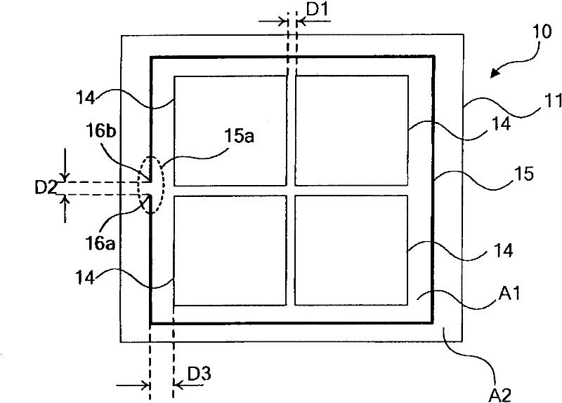
[0215] [Example 1: figure 1 Manufacture of liquid crystal display panel mounting substrates]

[0216] The following ingredients were mixed to prepare sealant a.

[0217] [Sealant a]

[0218] ·Bisphenol A type epoxy resin modified diacrylate resin 15 parts

[0219] 75 parts of methacrylic acid modified epoxy resin

[0220] · Filling 15 parts

[0221] ·Epoxy resin 10 parts

[0222] 5 parts of latent epoxy curing agent

[0223] ·Photofree radical polymerization initiator 2 parts

[0224] 10 parts of thermoplastic polymer

[0225] · Additive 1 part

[0226] The above-mentioned bisphenol A-type epoxy resin-modified diacrylate was used after performing the following purification treatment.

[0227] Bisphenol A epoxy resin-modified diacrylate (3002A manufactured by Kyoeisha Chemical Co., Ltd., molecular weight 600) was dissolved in toluene. The step of washing this solution with ultrapure water was repeated.

[0228] The aforementioned methacrylic acid-modified epoxy resin...

Embodiment 2

[0249] [Example 2: figure 1 Manufacture of liquid crystal display panel mounting substrates]

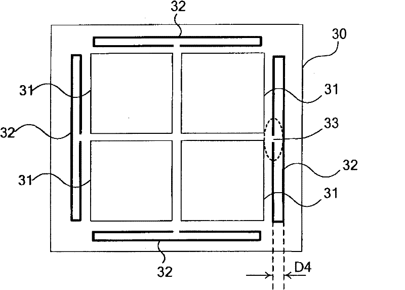
[0250] In the same manner as in Example 1, a sealant was applied to one substrate 11 to form four (two vertically and two horizontally) first frames 21 . Next, starting from the left side of the substrate, a sealant is applied so as to surround the above-mentioned four panels, thereby forming the second frame 22 . The second frame 22 is an annular substantially quadrangular shape, and one weather strip is removed at a width of about 10 mm in a linear portion of the quadrangular shape as a disconnection portion.

[0251] Next, in each first frame 21, four drops of liquid crystal 24 (liquid crystal MLC-11900-000 manufactured by Merck Co., Ltd.) were dropped for each frame to achieve a filling rate of 105%. Then, using a vacuum bonding apparatus (manufactured by Shin-Etsu Engineering Co., Ltd.), the liquid crystal-dropped substrate 11 and another substrate 27 of the same shape were st...

Embodiment 3

[0254] [Example 3: figure 2 Manufacture of liquid crystal display panel mounting substrates]

[0255] Using a screen printer (manufactured by Tokai Seiki Co., Ltd.), the first frame was provided on one substrate in the same manner as in Example 1. The line width of the first frame is 200 μm, and the cross-sectional area is 5000 μm 2 . Similarly, form figure 2 shown in the second box. The shape of the second frame was a rectangle with a length of 10 mm and a width of 55 mm, and a disconnection part was formed in a part. The second frame has a line width of 140 μm and a cross-sectional area of ​​3500 μm 2 .

[0256] Next, in each first frame, 2 drops of liquid crystal (liquid crystal MLC-11900-000 manufactured by Merck Corporation) were dropped on each frame so as to achieve a filling rate of 110%. Then, it was the same as that of Example 1 up to the step of curing the sealant by heating.

[0257] After pasting, D1 is 3.0mm, D2 is 0.2mm, and D3 is 2.0mm. The line widt...


PUM

PropertyMeasurementUnit
widthaaaaaaaaaa
softening pointaaaaaaaaaa
particle diameteraaaaaaaaaa

Abstract

The invention provides a liquid crystal panel mounting substrate in which the cell gap is uniform. The liquid crystal panel mounting substrate is produced as follows. A sealant is applied onto a substrate (11) to surround a pixel arrangement region to form a first seal (21) becoming a main seal. A sealant is arranged on the outer circumference of the first seal (21) to form a second seal (22) which is provided with disconnection portion (23) by uncoupling the one and the other end. A proper quantity of liquid crystal (24) is dripped to the inside of the first seal (21). The substrate (11) andanother substrate (27) are superimposed under reduced pressure. In this regard, the first seal (21) and the second seal (22) are not touched and the substrates face each other. The two substrates thus superimposed are then returned back to the atmospheric pressure from the reduced pressure. Inside of the second seal (22) which is the region of reduced pressure approaches gradually to the ambient atmospheric pressure through the disconnection portion (23). Since the substrates are stuck without generating a significant atmospheric pressure difference, distortion of the substrate is suppressed.Thereafter, the sealant is hardened to obtain a liquid crystal panel mounting substrate.

Description

technical field [0001] The present invention relates to a liquid crystal display panel mounting substrate and a manufacturing method thereof. Background technique [0002] Liquid crystal display panels are widely used in electronic equipment such as OA equipment and mobile phones due to their advantages of thinness, lightness, and low power consumption. A liquid crystal display panel is constructed by enclosing liquid crystal between two substrates bonded with a sealant, applying voltage to the liquid crystal to control the orientation of the liquid crystal, and modulating the light transmitted through the liquid crystal to display images. [0003] As a method of injecting liquid crystal between substrates, there are a liquid crystal injection method and a liquid crystal dropping method. In the liquid crystal injection method, an injection port for injecting liquid crystal is provided in a part of the weather strip formed on the substrate, and the liquid crystal is injected...

Claims


Application Information

Patent Timeline
Patent Type & Authority Patents(China)
IPC IPC(8): G02F1/1339C08L63/00
CPCG02F1/133351G02F1/1339C08G59/4035C08G59/08G02F2001/13415C08G59/1466G02F1/1341G02F1/13415C08L63/00
Inventor 水田康司中村健一五味俊一大塚裕明宫胁孝久
Owner MITSUI CHEM INC
Why Eureka
Try Eureka