Integrated devices with optical and electrical isolation and method for making

Active Publication Date: 2005-05-12
BAKER HUGHES INC
View PDF16 Cites 91 Cited by
  • Summary
  • Abstract
  • Description
  • Claims
  • Application Information

AI Technical Summary

Problems solved by technology

However, these solutions do not provide any optical isolation between adjacent devices.
In addition, a LOCOS structure usually leaves a wafer with a non-planar top surface, which can cause difficulties for subsequent fabrication processes.
Depending on the trench

Method used


Image

  • Integrated devices with optical and electrical isolation and method for making
  • Integrated devices with optical and electrical isolation and method for making
  • Integrated devices with optical and electrical isolation and method for making

Examples


Embodiment Construction

[0013] Reference will now be made in detail to exemplary embodiments of the invention, examples of which are illustrated in the accompanying drawings.

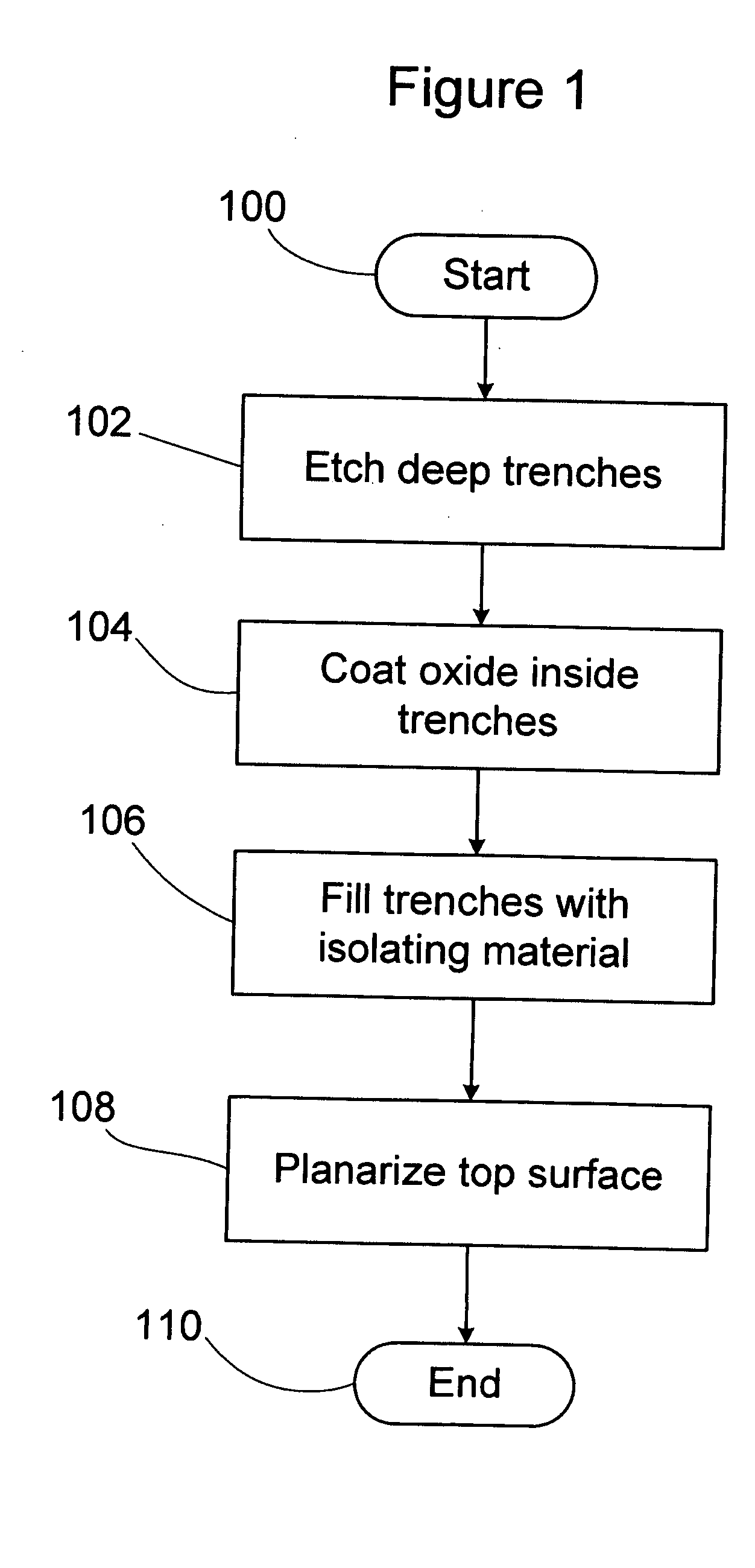
[0014]FIG. 1 is a flow chart illustrating a method for optical and electrical isolation between adjacent integrated devices according to an exemplary embodiment of the invention.

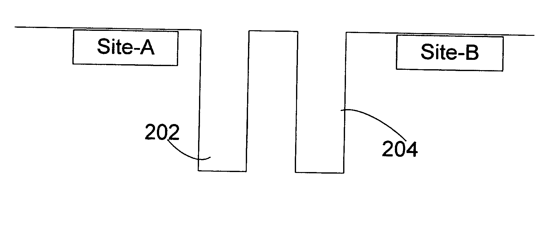
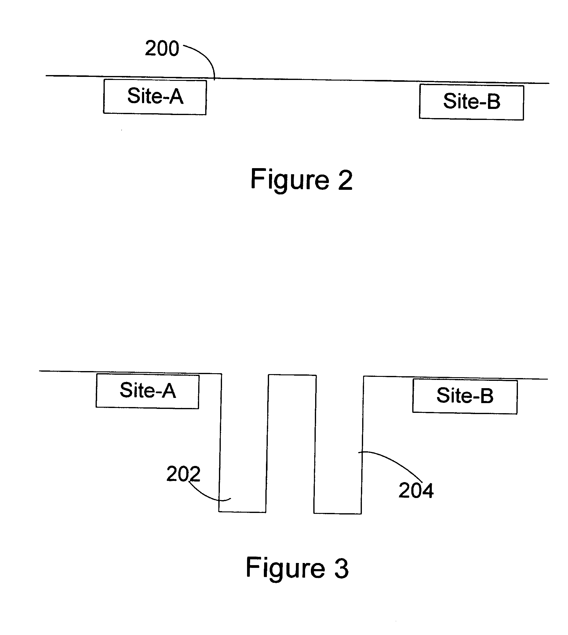
[0015] The process starts at step 100. The optical and electrical isolation method may be implemented, for example, on a piece of semiconductor wafer in which a plurality of integrated devices, such as photodiodes, photodetectors and other optical sensors, photoemitters, other electronic devices / circuits, and / or micro-electromechanical structures (MEMS) are to be fabricated. At step 100, there may be implant regions of different dopant types and doping density defined in the semiconductor wafer. Or future device sites in the wafer may be defined or identified in other manners known to those skilled in the art such as epitaxial layer formation.

[0016] At step ...


PUM


Abstract

The invention is directed to a method for optical and electrical isolation between adjacent integrated devices. The method comprises the steps of forming at least one trench through an exposed surface of a semiconductor wafer by removing a portion of the semiconductor wafer material, forming an electrically insulating layer on the sidewalls and the bottom of the at least one trench, filling the at least one trench by conformally depositing an optically isolating material, and planarizing the semiconductor wafer surface by removing the portion of the optically isolating material above the exposed surface of the semiconductor wafer.

Description

BACKGROUND OF THE INVENTION [0001] The present invention relates generally to the field of microelectronics and more particularly to a method and structure for optical and electrical isolation between adjacent integrated devices. [0002] Optical and electrical isolation between active devices is often an important requirement for integrated micro-systems, especially those involving optical sensors. A number of solutions to electrically isolate adjacent devices are available, including local oxidation of silicon (LOCOS), shallow trench isolation (STI) and deep trench isolation (DTI). When properly designed, these isolation structures can reduce unwanted diffusion of dopants, prevent and / or reduce capacitance coupling, or prevent latch-up between adjacent devices. However, these solutions do not provide any optical isolation between adjacent devices. In addition, a LOCOS structure usually leaves a wafer with a non-planar top surface, which can cause difficulties for subsequent fabricat...

Claims


Application Information

Patent Timeline
IPC IPC(8): H01L21/762H01L21/763H01L27/146
CPCH01L21/76224H01L27/14643H01L27/1463H01L21/763
Inventor KRETCHMER, JAMES WILLIAMFEDISON, JEFFREY BERNARDBROWN, DALE MARIUSSANDVIK, PETER MICAH
Owner BAKER HUGHES INC
Why Eureka
Try Eureka