Self light emission display device

a display device and light emission technology, applied in the direction of static indicating devices, identification means, instruments, etc., can solve the problems of reducing the light emission lifetime of the element, reducing the cost, and difficult to make the data drivers into one chip

Inactive Publication Date: 2005-05-19
TOHOKU PIONEER CORP
View PDF4 Cites 15 Cited by
  • Summary
  • Abstract
  • Description
  • Claims
  • Application Information

AI Technical Summary

Benefits of technology

[0018] The present invention has been developed as attention to the above-described problems has been paid, and it is an object of the present invention to provide a self light emission display dev

Problems solved by technology

In addition to this, an increase in the light emission drive current incurs a result that the light emission lifetime of the element is shortened.
Thus, it becomes difficult to make the data drivers into one chip, and a problem remains in terms of the cost.
In the case where the dual scan drive system is adopted as described above, although

Method used


Image

  • Self light emission display device
  • Self light emission display device
  • Self light emission display device

Examples


Embodiment Construction

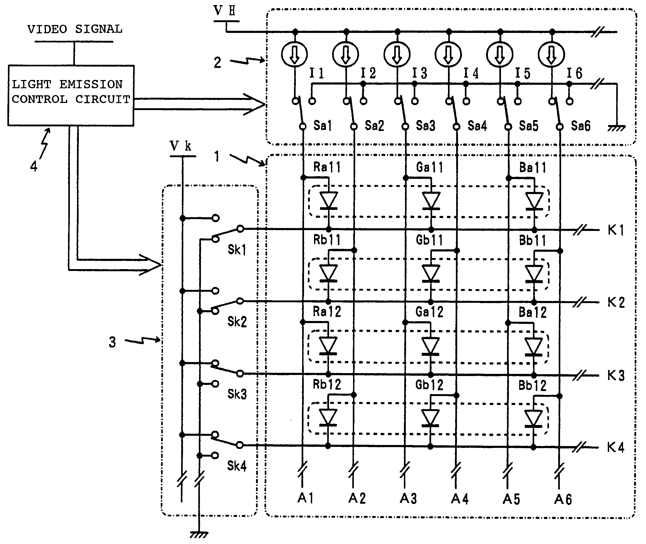
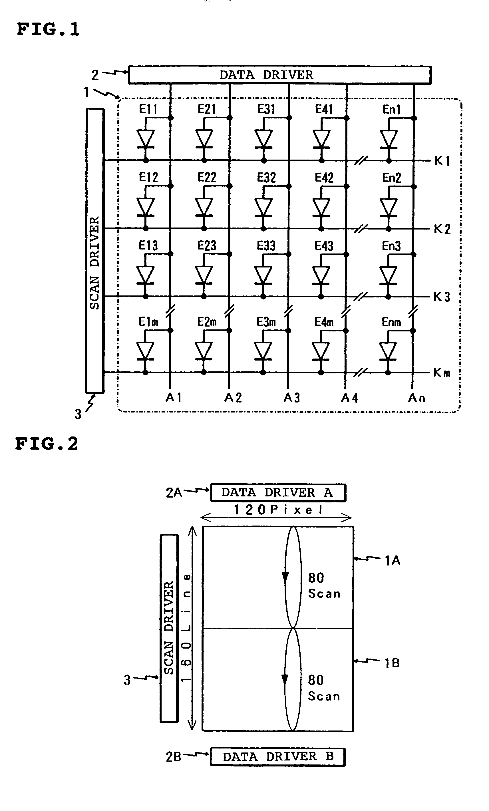
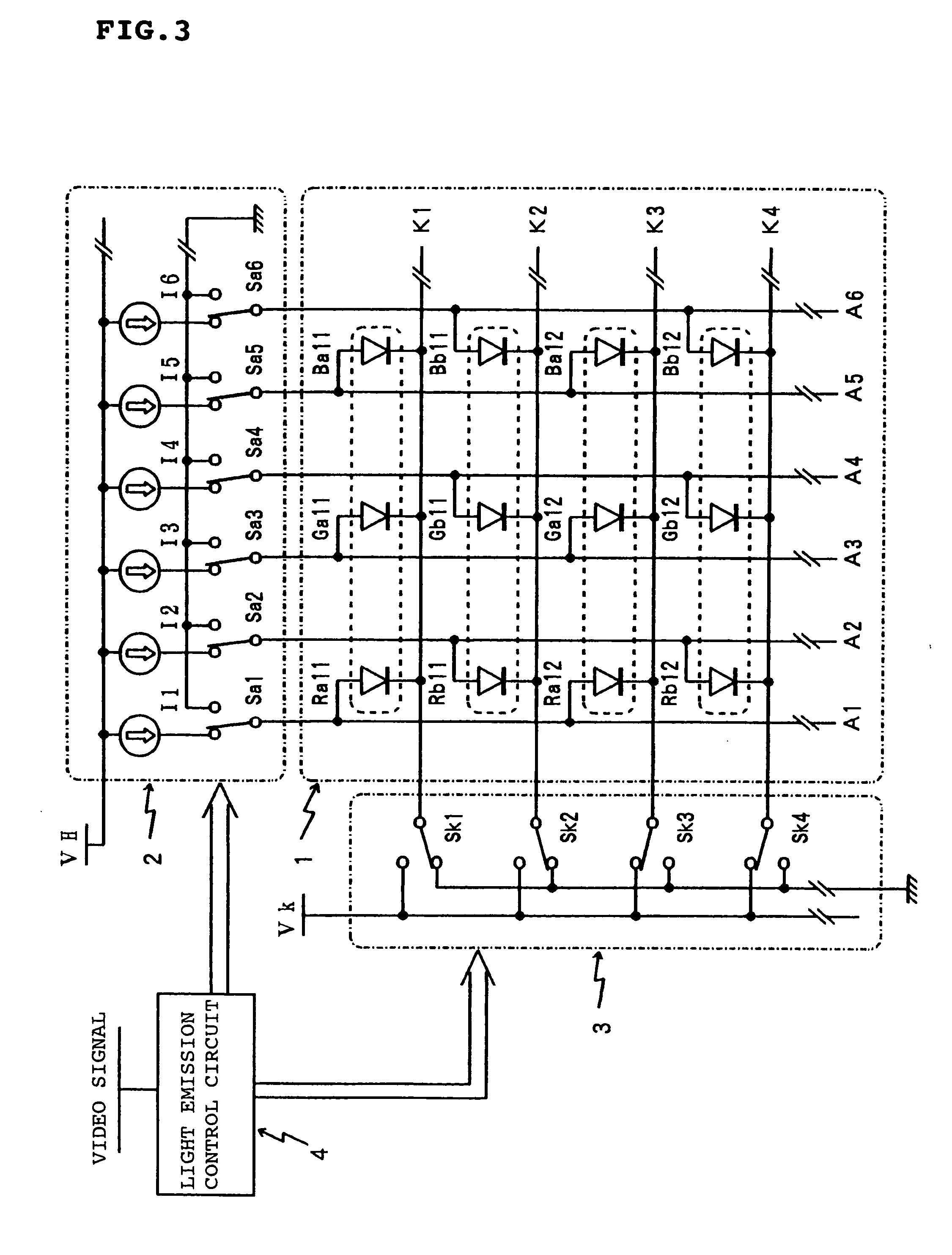
[0030] A self light emission display device according to the present invention will be described below with reference to an embodiment shown in FIGS. 3 and 4. First, FIG. 3 shows structures of a passive matrix type display panel and drive circuits therefor according to the present invention, and a display panel 1 shown in this FIG. 3 shows a form of a cathode line scan / anode line drive. Shown is a structure in which one pixel is formed while three subpixels that emit respective R (red), G (green), and B (blue) colors of light are grouped as surrounded by the broken line.

[0031] In the display panel 1 shown in FIG. 3, anode lines as data lines are arranged in a column (vertical) direction, and cathode lines as scan lines are arranged in a row (horizontal) direction. With respect to two adjacent anode lines, for example anode lines A1, A2, the anode terminal of an EL element Ra11 of red color light emission which is designated by the symbol of a diode is connected to one side anode li...


PUM


Abstract

A self light emission display device which substantially enables dual scan drive by one data driver comprises a plurality of scan lines K1, K2, . . . which are arranged in a horizontal direction, a plurality of data lines A1, A2, . . . which intersect these scan lines and are arranged in a vertical direction, and a plurality of light emitting elements Ra11, Rb11, . . . arranged on intersecting areas of the scan lines and the data lines. Cathode terminals of the light emitting elements whose anode terminals are connected respectively to the two adjacent data lines A1, A2 are connected to different scan lines one by one. Any two of the scan lines are selected for scanning simultaneously. Thus, since light emission duty of each EL element can also be approximately doubled, instantaneous light emission intensity of each EL element can be set low, and stress on the EL elements can be reduced. Further, since respective data lines can be drawn from one side end portion of the display panel, dual scan drive becomes substantially possible by one data driver.

Description

BACKGROUND OF THE INVENTION [0001] 1. Field of the Invention [0002] The present invention relates to a self light emission display device aimed at a passive matrix type display panel in which for example organic EL (electroluminescent) elements are employed as light emitting elements, and particularly to a self light emission display device which is suitable for forming a large size display panel. [0003] 2. Description of the Related Art [0004] A display panel constructed by arranging light emitting elements in a matrix pattern has been developed widely, and as the light emitting element employed in such a display panel, an organic EL element in which an organic material is employed in the light emitting layer thereof has attracted attention. This is because of backgrounds one of which is that by employing, in the light emitting layer of the element, an organic compound which enables an excellent light emission characteristic to be expected, a high efficiency and a long life which c...

Claims


Application Information

Patent Timeline
IPC IPC(8): G09F9/30H01L51/50G09G3/20G09G3/30G09G3/32H01L27/32H05B33/14
CPCG09G3/3216G09G3/3266G09G3/3275H01L27/3281G09G2300/0439G09G2310/0205G09G2310/0221G09G2300/0426H10K59/17G09G3/30G09G3/20
Inventor SEKI, SHUICHI
Owner TOHOKU PIONEER CORP
Why Eureka
Try Eureka