

Substrate processing apparatus
a processing apparatus and substrate technology, applied in the field of substrate processing apparatus, can solve the problems of affecting the cost of processing substrate, the price of the device, and the cost of producing electronics by the manufacturing cost of electronic devices
- Summary
- Abstract
- Description
- Claims
- Application Information
AI Technical Summary
Benefits of technology
Problems solved by technology
Method used
Image

Examples
Embodiment Construction
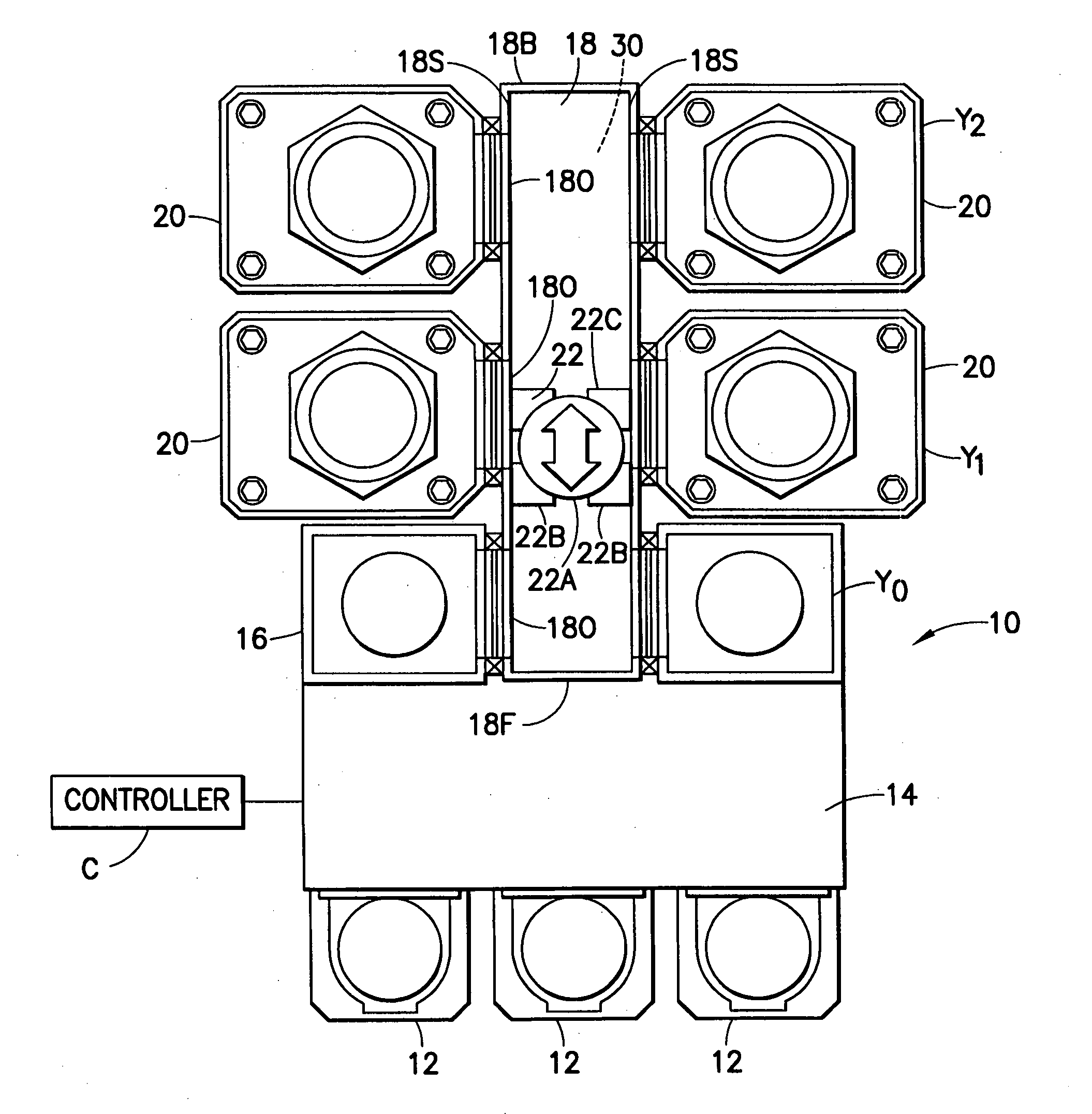
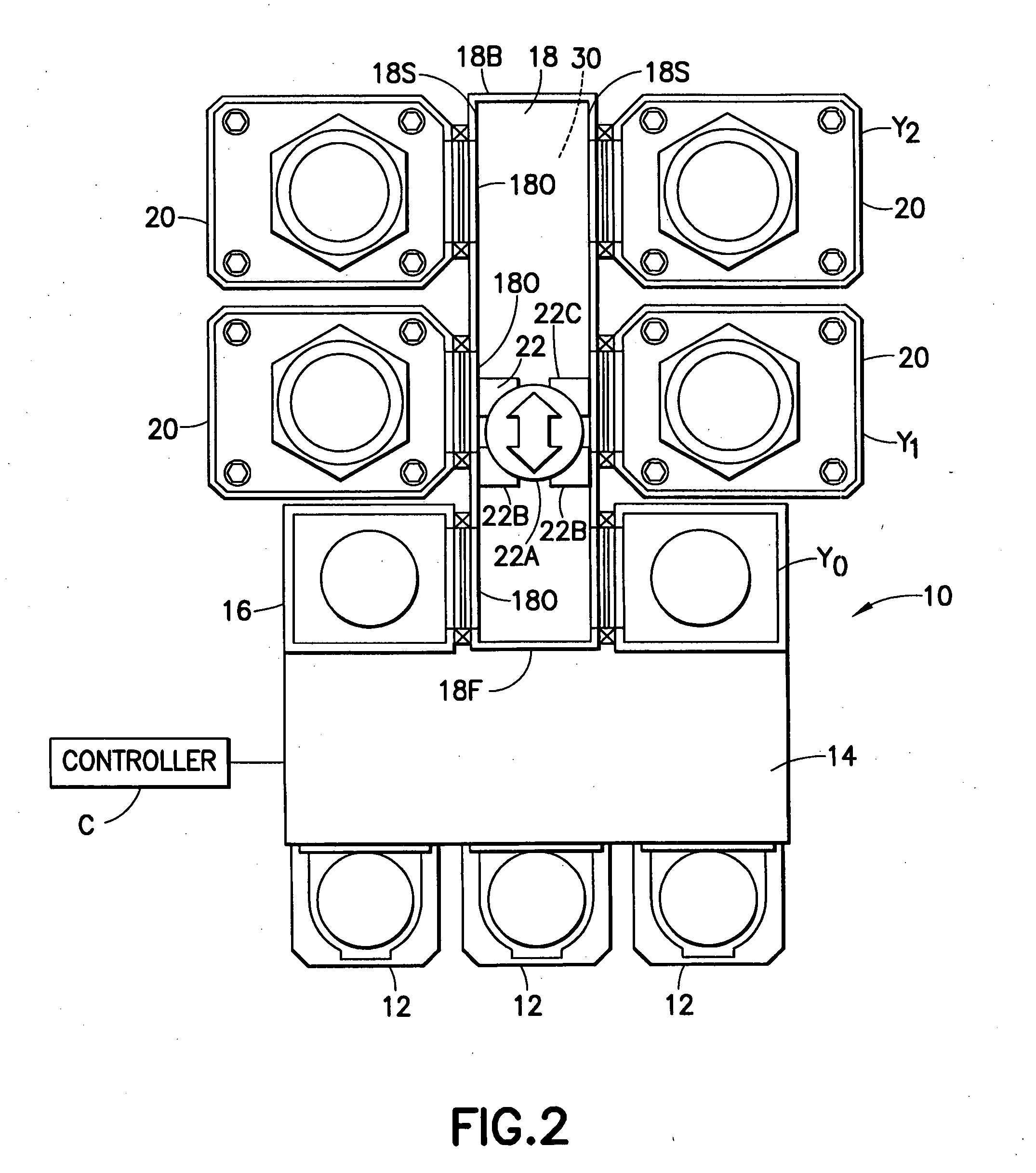
[0006] In accordance with the first embodiment, a substrate processing apparatus is provided. The apparatus comprises a transport chamber, at least one substrate holding module for holding a substrate, a transport vehicle, and another module. The transport chamber is capable of having a controlled atmosphere therein. The at least one substrate holding module is communicably connected to the transport chamber for allowing transfer of the substrate between the at least one holding module and the transport chamber. The transport vehicle, is movably mounted in the transport chamber. The vehicle has a base and a substrate transfer arm that is movably jointed and movably mounted to the base. The other module is capable of holding the substrate and is communicably connected to the transport chamber for transferring the chamber to the substrate therebetween. The transport chamber defines a linear travel slot for the vehicle. The at least one holding module is located on one side of the slot...
PUM
| Property | Measurement | Unit |
|---|---|---|
| angle | aaaaa | aaaaa |
| semi-conductor | aaaaa | aaaaa |
| size | aaaaa | aaaaa |
Abstract
Description
Claims
Application Information