Image display device

a display device and image technology, applied in the direction of identification means, static indicating devices, instruments, etc., can solve the problems of difficult to cancel a real-time variation in the characteristic, luminous brightness gradually varies, and the characteristic varies

Active Publication Date: 2005-05-26
SAMSUNG DISPLAY CO LTD +1
View PDF7 Cites 165 Cited by
  • Summary
  • Abstract
  • Description
  • Claims
  • Application Information

AI Technical Summary

Benefits of technology

[0018] In an aspect of the present invention, each of the pixels comprises an on / off control switch for stopping driving operation of the light emitting element provided in the pixel, a current measuring circuit connected to one end of the power line, a pixel current value storing circuit for storing a current value measured by the current measuring circuit, and a circuit for modulating the display signal using the measured current value stored in the pixel circuit value storing circuit.

Problems solved by technology

Ideally, the image display should be realized through the above operation without any trouble, but it actually involves a problem that luminous brightness gradually varies with deterioration of the light emitting element 213 with time passage.
Thus it is difficult to cancel a variation in the characteristic on a real time basis while a motion image is displayed.
However, from the fact that the characteristic of the light emitting element is sensitive to temperature, we noticed a problem that the characteristic varies with heat generated by the element itself on a real time basis.
Since such characteristic variation caused by the temperature change disappears in a certain time, it affects the image quality in the form of a sort of long-time after-image, thus deteriorating the stability of the luminous brightness.

Method used


Image

  • Image display device
  • Image display device
  • Image display device

Examples


embodiment 1

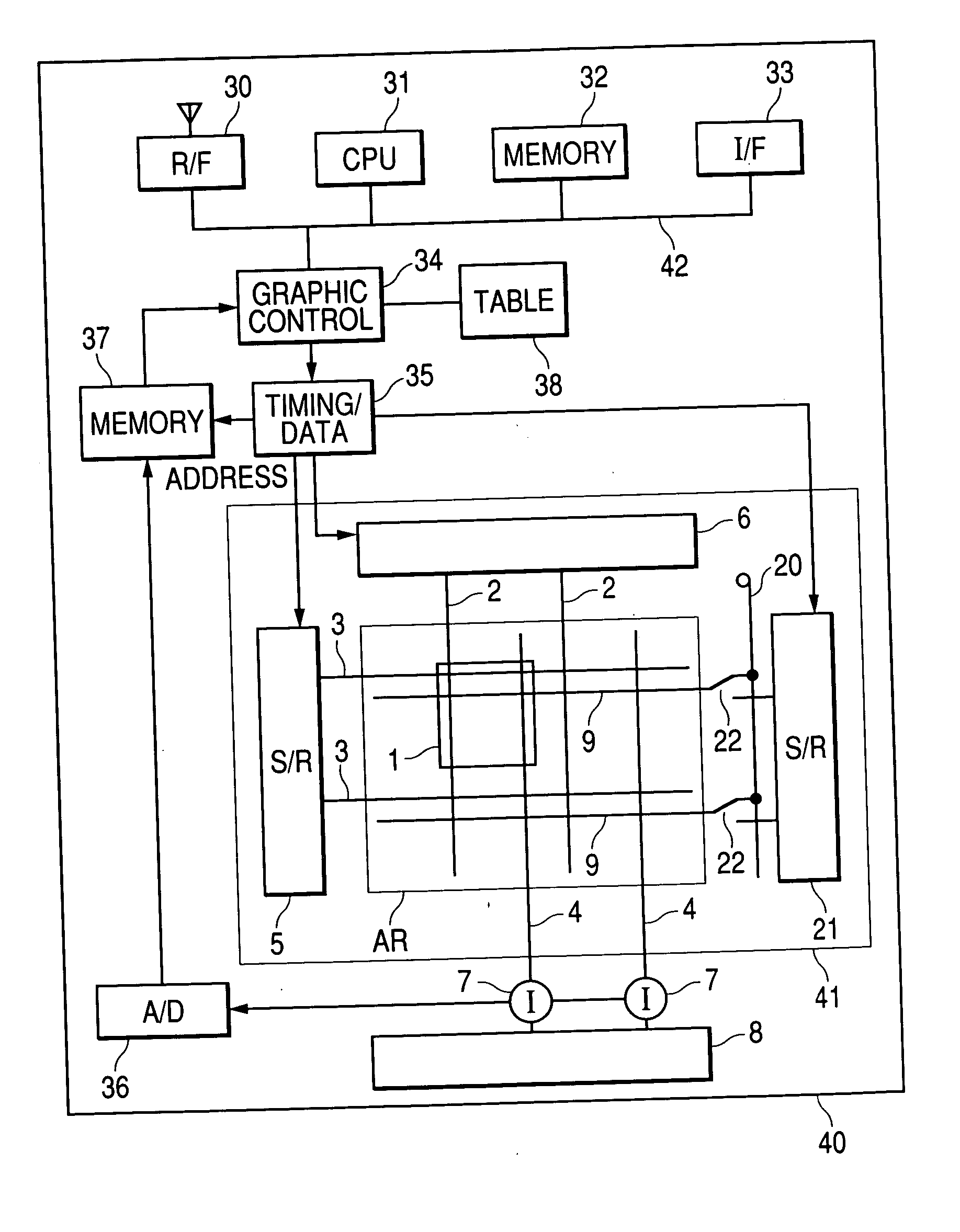
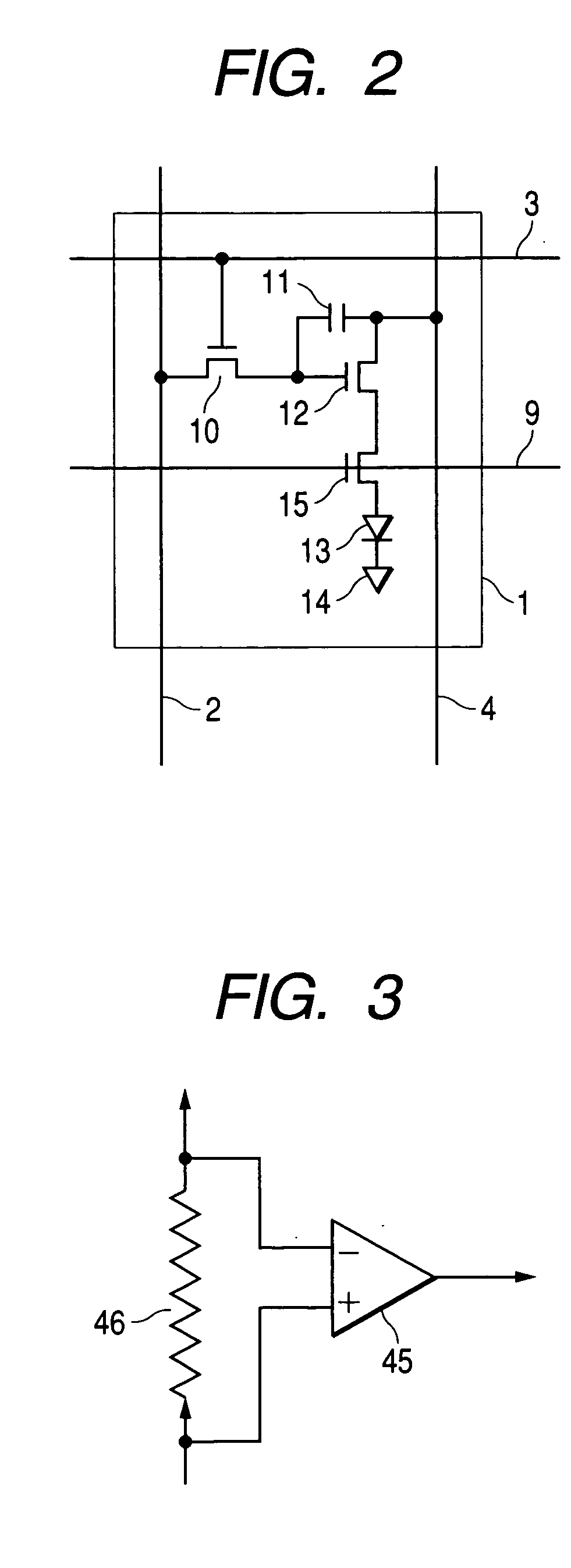
[0037]FIG. 1 shows an arrangement of a portable terminal 40 as an image display device in accordance with first embodiment of the present invention. Pixels 1 are provided in a display zone AR in the form of a matrix having rows and columns. Connected to each of the pixels 1 are a signal line 2, a gate line 3, a power line 4, and an on / off control line 9. Many of such pixels 1 are actually provided in the display zone AR, but only one of the pixels is shown in FIG. 1 for simplicity of the drawing. One end of the signal line 2 is connected to a signal voltage input circuit 6. One end of the gate line 3 is connected to a first shift register circuit 5. One end of the power line 4 is connected to a power supply circuit 8 via a current measuring circuit 7. One end of the on / off control line 9 is connected to a second shift register circuit 21 via an on / off changeover switch 22, and the other end of the on / off changeover switch 22 is connected to an on / off line 20. In this connection, the...

embodiment 2

[0051] A second embodiment of the present invention will be explained by referring to FIGS. 5 to 9. The present embodiment is basically the same as the embodiment 1 in the basic structure and operation, but is different from the embodiment 1 in a pixel circuit provided on a glass substrate and in a driving system therefor. Accordingly, attention will be directed only to the pixel circuit and the structure and operation thereof will be explained.

[0052]FIG. 5 is an arrangement of a pixel circuit in a portable terminal in accordance with a second embodiment of the present invention. Pixels 1A are provided in a display zone AR in the form of a matrix. A signal line 2,. a reset line 53, a power line 4, and an on / off control line 9 are connected to each pixel 1A. A multiplicity of such pixels 1A are actually provided in the display zone AR, but only one of the pixels is shown in FIG. 5 for simplicity of the drawing. One end of the signal line 2 is connected to a signal voltage input circ...

embodiment 3

[0070] Explanation will be made as to a third embodiment of the present invention by referring to FIGS. 10 and 11. The basic arrangement and operation. of a portable terminal in accordance with the third embodiment of the invention are substantially the same as those of the embodiment 1 already explained, and are different from those of the embodiment 1 only in the current measuring circuit and a driving system therefor. Thus, attention is directed only to the current measuring circuit part, and the structure and operation thereof will be explained.

[0071]FIG. 10 is an arrangement of a pixel zone part in a portable terminal to which the embodiment 3 of the invention is applied. Pixels 1B are provided in a display zone AR in the form of a matrix. A signal line 2, a gate line 3, a power line 4, and an on / off control line 9 are connected to each pixel 1B. A multiplicity of such pixels 1B are actually provided in the display zone AR, but only one of the pixels is shown in FIG. 10 for si...


PUM

PropertyMeasurementUnit
drive current characteristicsaaaaaaaaaa
drive currentaaaaaaaaaa
brightnessaaaaaaaaaa

Abstract

An image display device which has a stable luminous brightness among pixels. An on/off control switch 15 for stopping the driving operation of a light emitting element 13 is provided in a pixel 1. A change in the luminous brightness caused by a variation in the characteristic of the light emitting element 13 is suppressed by feeding a result measured by a current measuring circuit provided in one end of a power line 4 back to a drive signal for the light emitting element 13.

Description

INCORPORATION BY REFERENCE [0001] The present application claims priority from Japanese application JP 2003-392138 filed on Nov. 21, 2003, the content of which is hereby incorporated by reference into this application. BACKGROUND OF THE INVENTION [0002] The present invention relates to a high-quality image display device and more particular, to an image display device of a light-emitting flat-panel type such as organic electro-luminescence. [0003] There are various types of such flat-panel type image display devices including a liquid crystal display (LCD), a field emission display (FED), a plasma display panel (PDP), and an organic electro-luminescence (which will also be referred to merely as the organic EL, hereinafter) device, which go into actual use or are still in the research stage of actual use. Of these flat panel type image display devices, self light-emitting and light-emitting flat panel types, where pixel itself emits light, receive much attention. In the LCD or organi...

Claims


Application Information

Patent Timeline
Patent Type & Authority Applications(United States)
IPC IPC(8): H01L51/50G02F1/133G09F9/30G09G3/00G09G3/20G09G3/22G09G3/30G09G3/32G09G5/00H01L21/00H05B33/00H05B33/14
CPCG09G3/2014G09G3/3233G09G3/3258G09G2320/043G09G2300/0861G09G2310/066G09G2320/0295G09G2300/0842G09G3/30
Inventor AKIMOTO, HAJIMEKINUGAWA, KIYOSHIGEHAYASHI, NOBUAKI
Owner SAMSUNG DISPLAY CO LTD
Why Eureka
Try Eureka