Roughened bonding pad and bonding wire surfaces for low pressure wire bonding

a low-pressure wire bonding and bonding pad technology, applied in the direction of semiconductor devices, electrical equipment, semiconductor/solid-state device details, etc., can solve the problems of reducing the surface area of the bonding pad. , to achieve the effect of preventing damage to the semiconductor device undergoing processing and increasing the surface area

Active Publication Date: 2005-05-26
GLOBALFOUNDRIES US INC
View PDF21 Cites 22 Cited by
  • Summary
  • Abstract
  • Description
  • Claims
  • Application Information

AI Technical Summary

Benefits of technology

[0010] Bearing in mind the problems and deficiencies of the prior art, it is therefore an object of the present invention to provide a method and intermediate structure for wire bonding that avoids creating any excessive force and power applied during the formation of the wire bond such that any distortion, stress, and / or cracking of the bonding pad and / or underlying substrate material is avoided.
[0011] It is another object of the present invention to provide a method and intermediate structure for wire bonding that generate strong, reliable wire bonds.
[0012] Another object of the present invention is to provide a method and intermediate structure for wire bonding that provide wire bonds without requiring any excessive force, temperature and energy applied during the formation of the wire bond.

Problems solved by technology

These conventional bonding techniques are often dependent upon a variety of processing conditions including, but not limited to, mechanical pressure, temperature, strength of the electrode or bond pad, power level of the added ultrasonic excitation, time, and so forth whereby any of such processing conditions can ultimately lead to semiconductor failure.
For example, compression of the small, rigid ball at the end of the bonding wire often leads to structural damage and / or deformation of the substrate being compressed.
However, this method of attaching wire bonding via thermocompression can undesirably result in forces that are capable of causing distortion, stress, and / or cracks in the pad, electrode or underlying substrate.
Further, wherein the substrate being processed includes a low-k dielectric material, it is commonly known that such materials have poor mechanical strength, and as such, are highly susceptible to damage and / or cracking during any conventional wire bonding technique.
This is typically a result of the insertion of a wire bond being inserted with an excessive force during the bonding process, which leads to distortion, stress, and / or cracking of the bonding pad or any other underlying substrate material.
In turn, any cracks, stresses and / or distortions in the bonding pad or any other underlying layer jeopardize the strength of the resultant bond and / or device reliability.

Method used


Image

  • Roughened bonding pad and bonding wire surfaces for low pressure wire bonding
  • Roughened bonding pad and bonding wire surfaces for low pressure wire bonding
  • Roughened bonding pad and bonding wire surfaces for low pressure wire bonding

Examples


Embodiment Construction

)

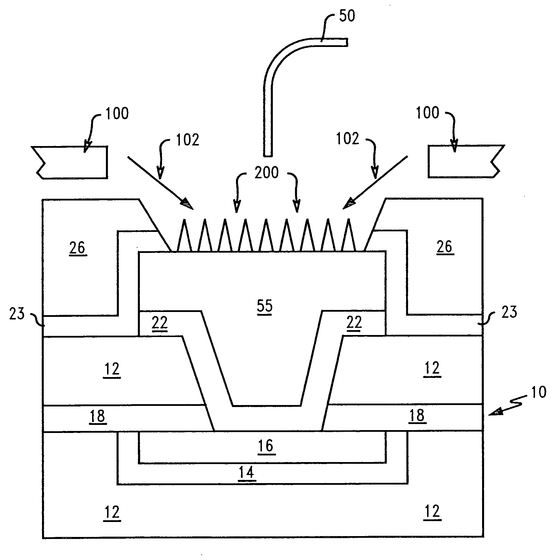
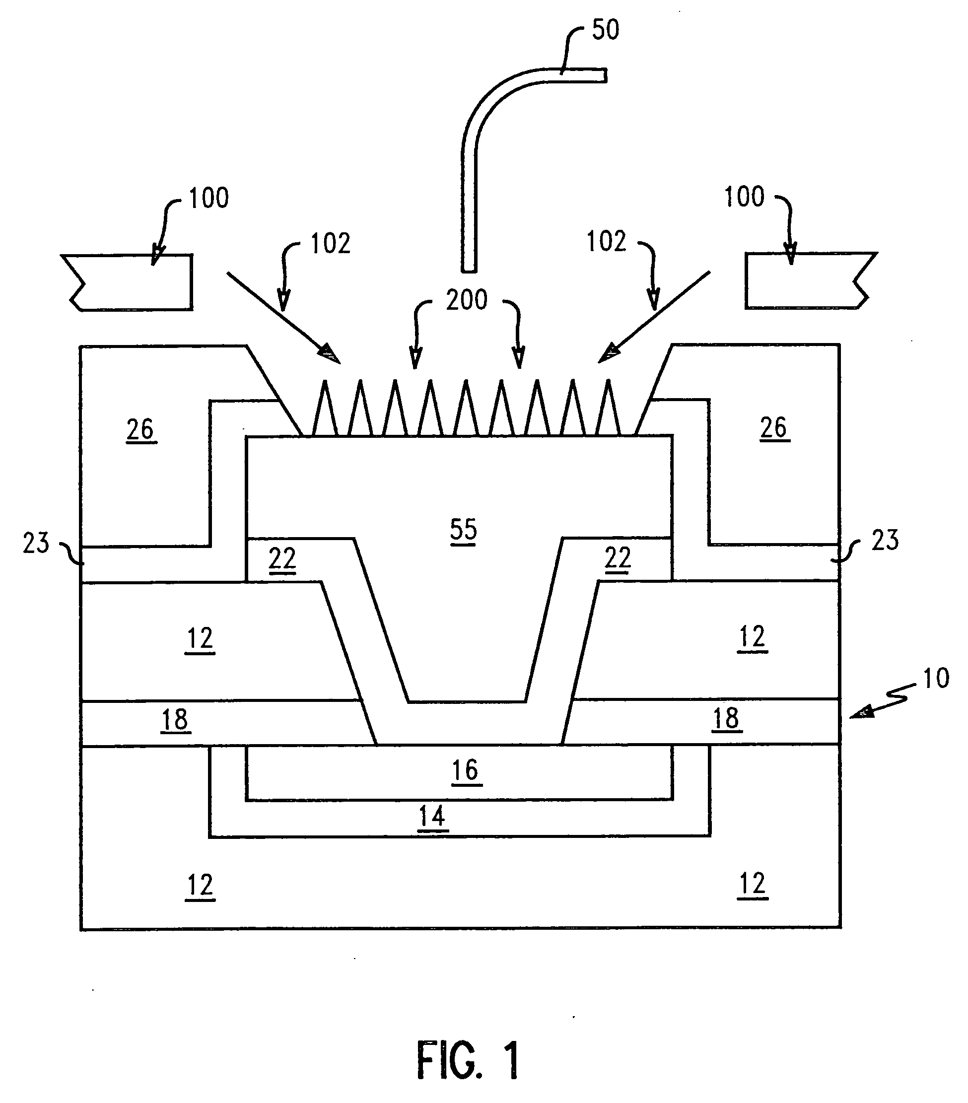
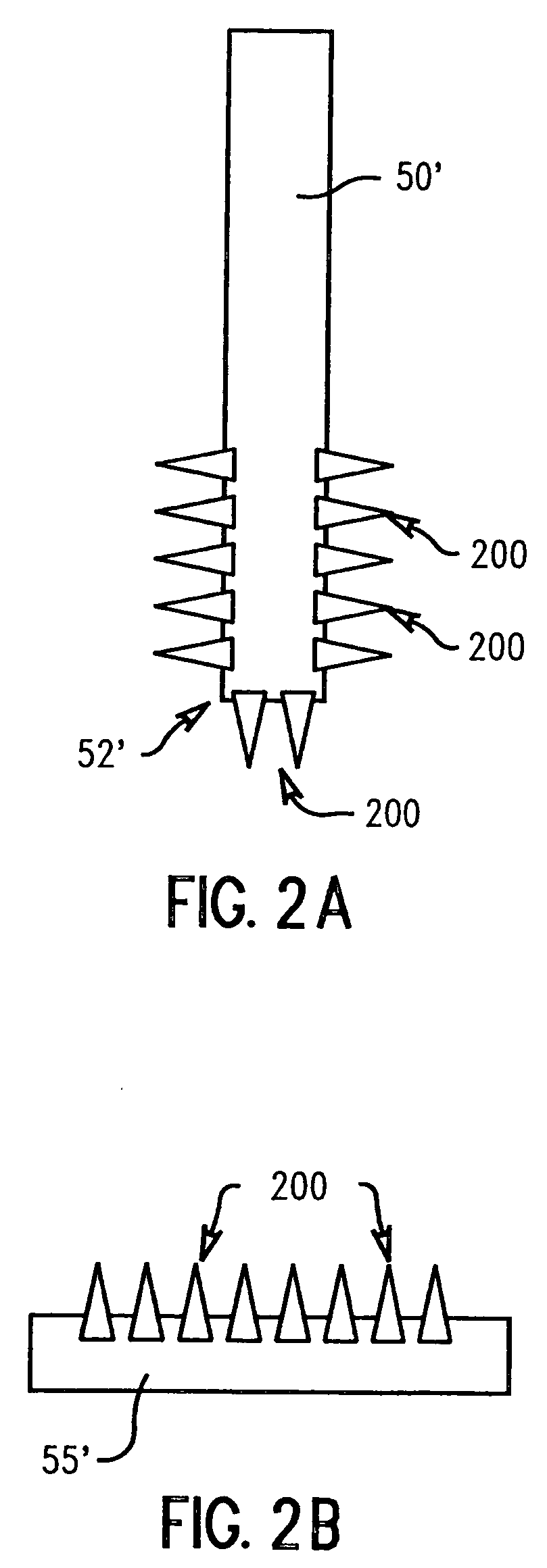
[0035] In describing the preferred embodiment of the present invention, reference will be made herein to FIGS. 1-3D of the drawings in which like numerals refer to like features of the invention.

[0036] Dielectrics have poor mechanical strength and are subject to cracking. Wire bonding to a semiconductor can induce cracks / damage in the dielectric when stresses are applied, which can ultimately lead to semiconductor failure. The present invention details a structure and method for low-pressure wire bonding to reduce the propensity of dielectric materials, particularly low-k dielectric materials, to mechanical failure.

[0037] In accordance with the invention, an approach is herein presented to increase the reactivity between the bond wire and the bond pad, which reduces the amount of pressure and ultrasonic and thermal energy required for wire bonding processing. In so doing, the invention discloses a roughened surface structure and methodology approach for low-pressure wire bonding ...


PUM

PropertyMeasurementUnit
roughnessaaaaaaaaaa
roughnessaaaaaaaaaa
roughnessaaaaaaaaaa

Abstract

An intermediate semiconductor structure and method for low-pressure wire bonding that reduces the propensity of dielectric material to mechanical failure due to any wire bonding stresses. Roughened surfaces such as metal pillars or metal dendrites are provided on a bonding pad, bonding wire or both. These roughened surfaces increase reactivity between the bond wire and the bond pad to form strong bonds. This increased activity as a result of the roughened bonding pad and / or wire surfaces reduce the amount of pressure, temperature and energy required for wire bonding, which in turn, avoids damage to the bonding pad as well as the semiconductor substrate.

Description

BACKGROUND OF THE INVENTION [0001] 1. Field of the Invention [0002] The present invention relates to semiconductor substrates, and more particularly, to low-pressure wire bonding methods and apparatus that reduce the propensity of low-k dielectric materials of mechanical failure due to wire bonding stresses. [0003] 2. Description of Related Art [0004] In semiconductor surface mount technology, integrated circuits (ICs) typically have one or more semiconductor-based circuits wired by metal interconnects, which in turn, have terminal inputs and outputs (I / O) to external circuitry. These ICs are often mounted on a mounting area of a lead frame having leads. Each I / O terminal is then connected to a lead by a thin bonding wire, which is typically made of gold or aluminum. [0005] In making interconnections within an IC, each region of the semiconductor is provided with an electrode for connection with the bonding wire for connecting regions of the IC to each other. For those connections h...

Claims


Application Information

Patent Timeline
Patent Type & Authority Applications(United States)
IPC IPC(8): H01L21/00H01L21/44H01L21/60H01L23/485
CPCH01L24/05H01L2224/04042H01L24/48H01L24/85H01L2224/05073H01L2224/05166H01L2224/05187H01L2224/05556H01L2224/05624H01L2224/05644H01L2224/05647H01L2224/45124H01L2224/45144H01L2224/4807H01L2224/85205H01L2224/85345H01L2224/85365H01L2224/85385H01L2924/01006H01L2924/01013H01L2924/01022H01L2924/01027H01L2924/01028H01L2924/01029H01L2924/01031H01L2924/01046H01L2924/01047H01L2924/0105H01L2924/01074H01L2924/01078H01L2924/01079H01L2924/01082H01L2924/04953H01L2924/14H01L24/45H01L2224/48647H01L2224/48644H01L2924/01019H01L2924/01024H01L2924/01033H01L2224/48724H01L2224/48747H01L2224/48624H01L2924/00014H01L2924/04941H01L2924/00H01L2224/48744
Inventor FITZSIMMONS, JOHN A.GAMBINO, JEFFREY P.WALTON, ERICK G.
Owner GLOBALFOUNDRIES US INC
Why Eureka
Try Eureka