Light receiving or emitting semiconductor apparatus

a technology of light-emitting semiconductors and semiconductor modules, which is applied in the direction of electrical devices, semiconductor devices, photovoltaic energy generation, etc., can solve the problems of large semiconductor modules, increased manufacturing costs, and increased manufacturing costs, and achieves the effect of lessening the brightness of light radiated from the emission sour

Inactive Publication Date: 2005-06-09
SPHELAR POWER
View PDF9 Cites 14 Cited by
  • Summary
  • Abstract
  • Description
  • Claims
  • Application Information

AI Technical Summary

Benefits of technology

[0015] When this semiconductor apparatus is a light-emitting semiconductor apparatus, the light generated from the substantially spherical pn junction is radiated in substantially all directions, and is radiated to the outside from the spherical or partial-spherical outer surface of the outer shell member. Because the outer shell member covers the outside of the spherical semiconductor device with a light-transmitting wall component whose thickness is at least ¼ the diameter of the spherical semiconductor device, the outer shell member exhibits a light diffusion function, the size of the light emission source is increased, the brightness of the light radiated from the emission source is lessened, and a softer light is radiated to the outside.

Problems solved by technology

However, the semiconductor module in U.S. Pat. No. 6,204,545 employs a structure in which the electrodes of the semiconductor cells are connected so that a plurality of semiconductor cells are connected in series, and these serial connections are arrayed in a plurality of planar rows, and the pair of electrodes of each semiconductor cell is extremely small, so when the above-mentioned serial / parallel connection structure is employed, manufacture becomes complicated, it is difficult to produce a large semiconductor module, and the cost of manufacturing a semiconductor module rises.
Because so many of the spherical semiconductor devices are required in this case, manufacturing expense become higher.
However, the position and orientation of the condensing lens must be varied according to the incident direction of the sunlight, and also a complex and expensive mechanism is needed to movably support and control the orientation of the condensing lens, so this situation is impractical.
Meanwhile, in the case of a light emitting panel used for lighting or display, the light emitted from the small-diameter spherical semiconductor device tends to be excessively bright, and it is difficult to construct a light emitting panel that emits soft light of the proper brightness.

Method used


Image

  • Light receiving or emitting semiconductor apparatus
  • Light receiving or emitting semiconductor apparatus
  • Light receiving or emitting semiconductor apparatus

Examples


embodiment 1 (see figs.15 to 17)

Other Embodiment 1 (See FIGS. 15 to 17)

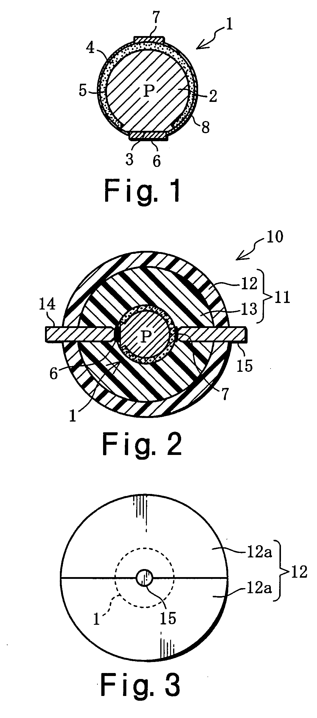
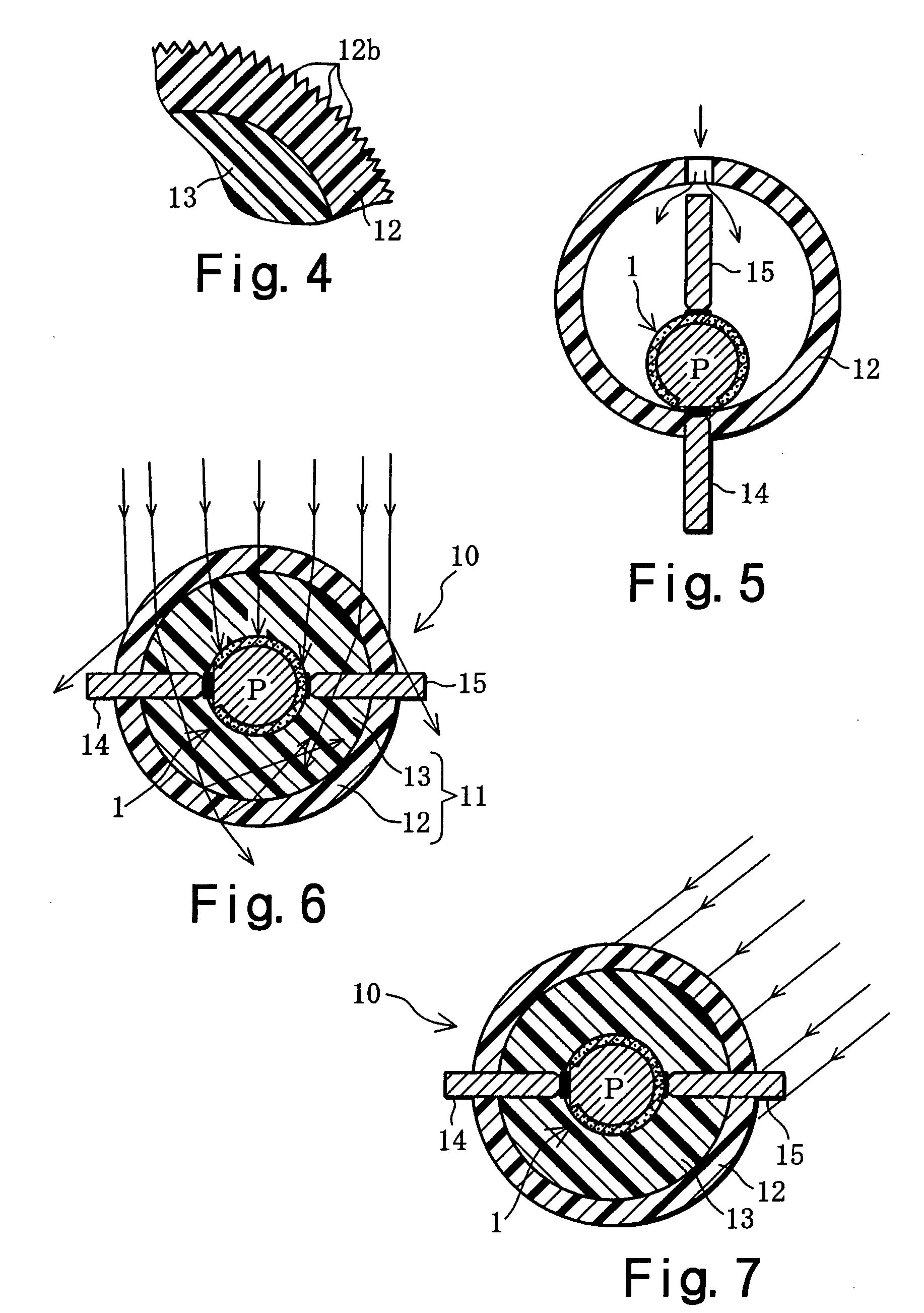
[0075] Next, descriptions will be made on another embodiment of a solar panel 50 in which many of the solar cells 1 are incorporated. This solar panel 50 corresponds to a semiconductor apparatus. With the solar panel 50 shown in FIGS. 15 to 17, a plurality of spherical solar cells 1 are arrayed in a matrix of a plurality of rows and a plurality of columns, a conduction connection mechanism is provided for electrically connecting in parallel the plurality of solar cells 1 in each row or column, and there is provided an outer shell member 51 comprising a plurality of substantially spherical outer shell components 52 that cover the plurality of solar cells 1, and a flat component 53 formed integrally with the plurality of outer shell components 52.

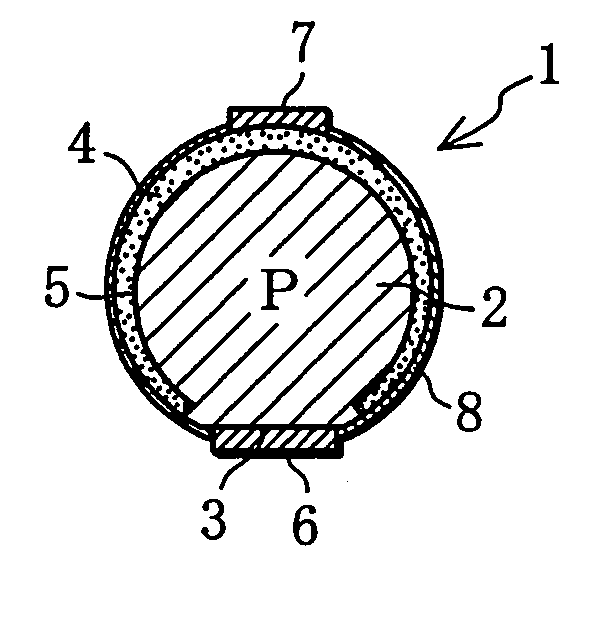
[0076] The solar cells 1 are located at the center of the outer shell components 52, the outer shell components 52 cover the outer surface of the solar cells 1 with a light-transmitting wall component, ...

embodiment 2 (see figs.18 to 21)

Other Embodiment 2 (See FIGS. 18 to 21)

[0083] Next, descriptions will be made on a solar panel 60 in which many of the solar cells 1 are incorporated into a solar string 61, and these are assembled into panel form. This solar string 61 corresponds to a semiconductor apparatus, and this solar panel 60 also corresponds to a semiconductor apparatus.

[0084] As shown in FIGS. 18 and 19, the solar panel 60 comprises a case 62 made of a transparent synthetic resin, and five (for example) solar strings 61 housed in this case 62. The case 62 consists of five integrally-molded, substantially cylindrical string holders 63 capable of holding the solar strings 61, and a flange 64 is formed at the lower end of each of the string holders 63. As shown in FIGS. 20, 21, the solar strings 61 have a plurality of spherical solar cells 1 arranged in a column, a conduction connection mechanism 65 for connecting these solar cells 1 in parallel, and an outer shell member 66 that has a cylindrical outer surf...


PUM


Abstract

With a solar ball 10 serving as a light-receiving semiconductor apparatus, the outer surface of a spherical solar cell 1 is covered with a light-transmitting outer shell member 11, and electrode members 14, 15 are connected to electrodes 6, 7 of the solar cell 1. The outer shell member 11 comprises a capsule 12 produced by bonding together two halves, and a filler 13 that is packed inside this capsule and cured. A solar panel can be configured such that a plurality of the solar balls 10 are arrayed in a matrix and connected in parallel and in series, or a solar panel can be configured such that a multiplicity of spherical solar cells 1 are arrayed in a matrix and covered with a transparent outer shell member. A solar string in the form of a rod or cord can be configured such that a plurality of the solar cells 1 are arrayed in columns and connected in parallel, and then covered with a transparent outer shell member. Since the outer shell member 11 condenses light, the light-receiving area of the solar cell 1 can be expanded. Also discussed is a light-emitting semiconductor apparatus in which a spherical semiconductor device with a light-emitting function, rather than the solar cell 1, is covered with an outer shell member.

Description

TECHNICAL FIELD [0001] The present invention relates to a light-receiving or light-emitting semiconductor apparatus, and more particularly relates to an apparatus in which the outside of a spherical semiconductor device with a light-receiving or light-emitting function is covered with a light-transmitting outer shell member so as to improve the light condensation performance or light radiation performance. This can be used in various applications such as solar cells, lighting devices, and display devices. BACKGROUND OF THE INVENTION [0002] Conventionally, research has been directed toward a technology forming a pn junction via a diffusion layer on the surface of a small-diameter spherical semiconductor element composed of a p or n type semiconductor, connecting many of these spherical semiconductor elements in parallel to a common electrode, and putting to practical use for a solar cell or semiconductor photocatalyst. [0003] U.S. Pat. No. 3,998,659 discloses a solar cell configured ...

Claims


Application Information

Patent Timeline
Patent Type & Authority Applications(United States)
IPC IPC(8): H01L25/075H01L31/0216H01L31/00H01L31/0352H01L31/048H01L31/052H01L33/00H01L33/32
CPCH01L25/0753H01L31/02168H01L31/035281H01L31/03529H01L31/042H01L31/048H01L31/02008H01L33/24Y02E10/52H01L2924/1017H01L2224/16245H01L31/0547H01L33/20
Inventor NAKATA
Owner SPHELAR POWER
Why Eureka
Try Eureka