Solar cell and method for producing the same

Inactive Publication Date: 2005-06-16
SHARP KK
View PDF5 Cites 96 Cited by
  • Summary
  • Abstract
  • Description
  • Claims
  • Application Information

AI Technical Summary

Benefits of technology

[0014] In view of the foregoing, it is an object of the present invention to provide a solar cell having fine solar cel

Problems solved by technology

However, where the substrate is of polycrystalline silicon, this method can not significantly reduce the surface reflectivity thereof because polycrystalline silicon has various plane directions.
The irregularities formed on the substrate, however, have pointed tips and thus, a pn junction provided under a light-receiving surface of the substrate may be destroyed at heating of a metal paste for the formation of electrodes.
The gas etching using ClF3, as described above, may greatly reduce the reflectivity of the substrate surface.
However, as a result of a detailed examination of the gas-etched surface of the substrate by SEM (Scanning Electron Microscope), it is found that a number of small pores are formed in the surface, i.e., the surface is porous as shown in the SEM photograph of FIG. 17(a), owing to the irregularities being too microscopic.
If alkaline etching conditions are changed for removing the pores formed in the substrate surface, the low-reflectivity of the substrate surface can not be maintained.
From these facts, it is understood that maintaining the low-reflectivity of the substrate surface and removing the pores formed in the substrate surface are two contradictory objects to be achieved, and thus, realization of these two objects in one device is extremely difficult.

Method used


Image

  • Solar cell and method for producing the same
  • Solar cell and method for producing the same
  • Solar cell and method for producing the same

Examples


embodiment 1

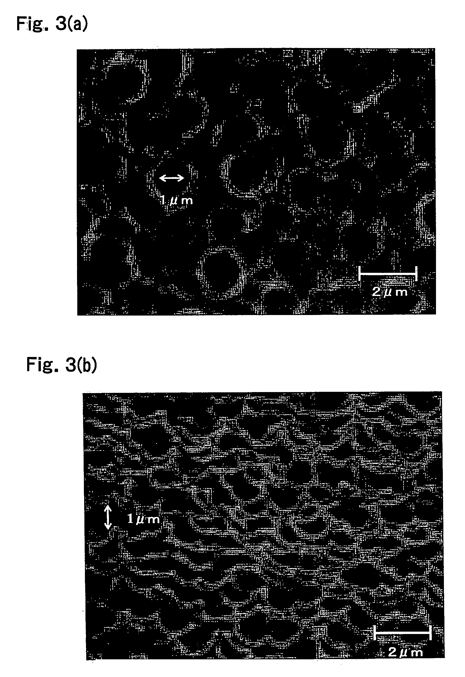
[0072]FIG. 3(a) and FIG. 3(b) are a top SEM image and a 60-degree oblique SEM image, respectively, of a plurality of depressions having a first type of configuration and size formed in surfaces of the substrate of

embodiment 2

[0073]FIG. 4(a) and FIG. 4(b) are a top SEM image and a 60-degree oblique SEM image, respectively, of a plurality of depressions a second type of configuration and size formed in surfaces of the substrate of

embodiment 3

[0074]FIG. 5(a) and FIG. 5(b) are a top SEM image and a 60-degree oblique SEM image, respectively, of a plurality of depressions having a third type of configuration and size formed in surfaces of the substrate of

[0075]FIG. 6 is a graph showing the surface reflectivity of the polycrystalline silicon substrates according to Embodiments 1 to 3 and the comparative example.

[0076] Shown in Table 1 are IV characteristics of the solar cells according to Embodiments 1-3 and the comparative example. In Table 1, Jsc indicates short-circuit current, Voc indicates open-circuit voltage and FF indicates fill factor and Pmax indicates maximum power.

TABLE 1Jsc (mA / cm2)Voc (V)FFPmax (W)Embodiment 130.60.5950.7782.19Embodiment 229.90.5940.7612.11Embodiment 329.70.5910.7692.11Comparative Example29.90.5950.7382.06

[0077] According to Table 1, the solar cell of Embodiment 1 is higher in all of the parameters except open-circuit voltage when compared to that of the comparative example. Further, the cel...


PUM


Abstract

A solar cell includes at least: a semiconductor substrate having a pn junction and a plurality of microscopic depressions formed in a light-receiving surface thereof; a front electrode formed on the light-receiving surface of the substrate; and a rear electrode formed on a rear surface of the substrate. The plurality of depressions each have a ratio of the maximum depth to the maximum diameter of 0.5 to 2.

Description

CROSS-REFERENCE TO RELATED APPLICATION [0001] This application is related to Japanese Patent Application No. 2003-389490 filed on Nov. 19, 2003, whose priority is claimed under 35 USC §119, the disclosure of which is incorporated by reference in its entirety. BACKGROUND OF THE INVENTION [0002] 1. Field of the Invention [0003] The present invention relates to a solar cell and a method for producing the same, and more particularly, to a method of forming irregularities on a surface of a silicon semiconductor substrate for reducing reflection of light incident on the surface. [0004] 2. Description of Related Art [0005] In order to improve photoelectric conversion efficiency, conventional solar cells have been constructed to have a plurality of irregularities on a surface of a semiconductor substrate. This allows light reflected at the surface of the substrate to be incident on the surface again, so that reflection losses can be reduced. Where the solar cells are formed using a (100)-or...

Claims


Application Information

Patent Timeline
IPC IPC(8): H01L31/04H01L31/00H01L31/0236
CPCY02E10/547H01L31/02363
Inventor HAYASHIDA, SHIGEKI
Owner SHARP KK
Why Eureka
Try Eureka