Optical element, lens unit, imaging module, electronic apparatus, and method of manufacturing optical element

Inactive Publication Date: 2016-12-22
FUJIFILM CORP
View PDF0 Cites 11 Cited by
  • Summary
  • Abstract
  • Description
  • Claims
  • Application Information

AI Technical Summary

Benefits of technology

[0021]According to the present invention, it is possible to provide an optical lens capable of reducing surface reflection on a light blocking layer so as to avoid ghosting,

Problems solved by technology

It can be expected that it will become more and more difficult to cope with this demand in the future.
This returning light is highly likely to be r

Method used


Image

  • Optical element, lens unit, imaging module, electronic apparatus, and method of manufacturing optical element
  • Optical element, lens unit, imaging module, electronic apparatus, and method of manufacturing optical element
  • Optical element, lens unit, imaging module, electronic apparatus, and method of manufacturing optical element

Examples


Example

EXPLANATION OF REFERENCES

[0034]100: imaging module[0035]11: imaging section[0036]110: lens unit[0037]15: optical lens[0038]16: light blocking layer[0039]18: lens base member[0040]18A: lens base member main body[0041]18B: AR coat

DESCRIPTION OF THE PREFERRED EMBODIMENTS

[0042]Hereinafter, embodiments of the present invention will be described with reference to drawings.

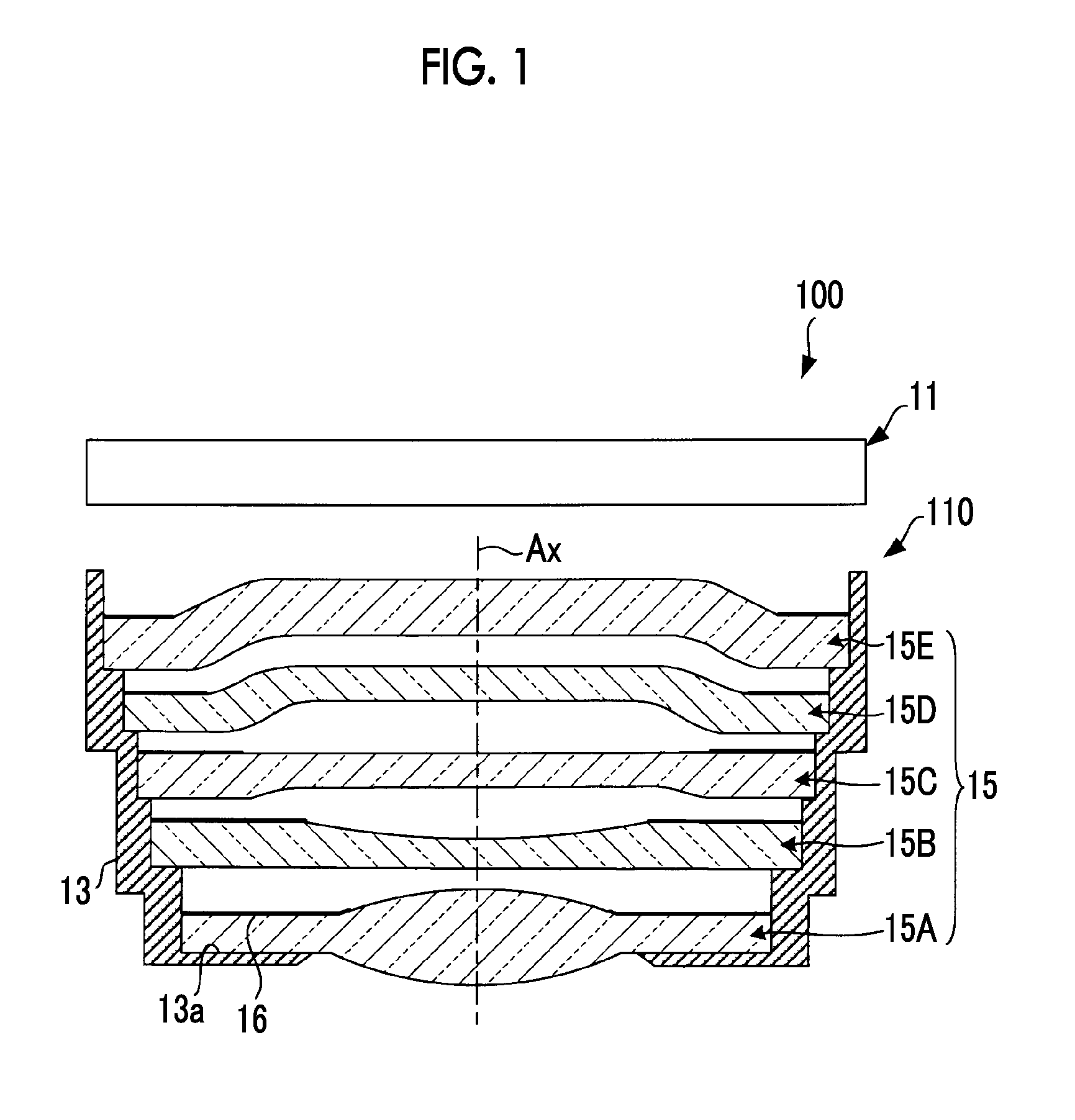
[0043]FIG. 1 is a schematic sectional view illustrating an imaging module according to an embodiment of the present invention.

[0044]An imaging module 100 has a lens unit 110 and an imaging section 11 that includes an imaging element for capturing an image of a subject through the lens unit 110, and is disposed in a casing of an electronic apparatus such as a smartphone or a digital camera supported by a supporting member such as a substrate which is not shown.

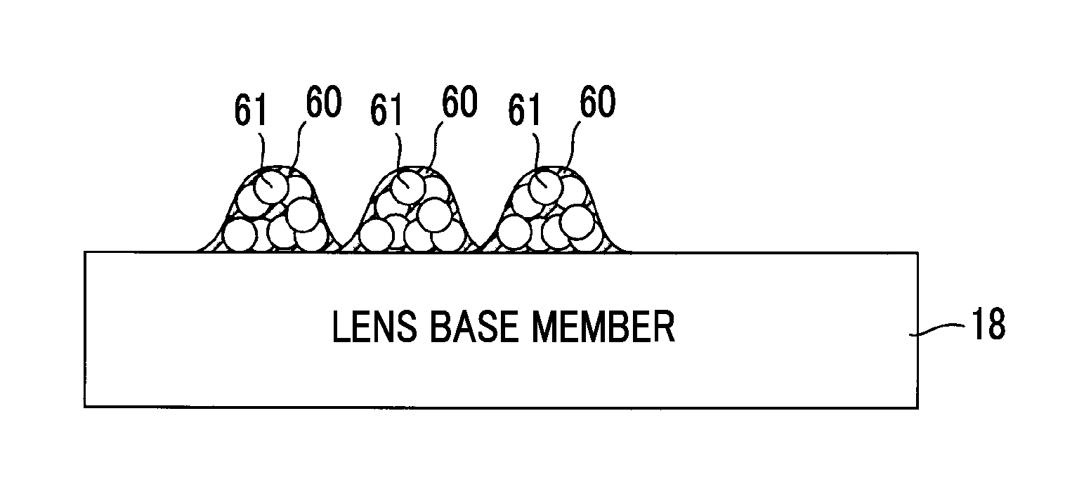
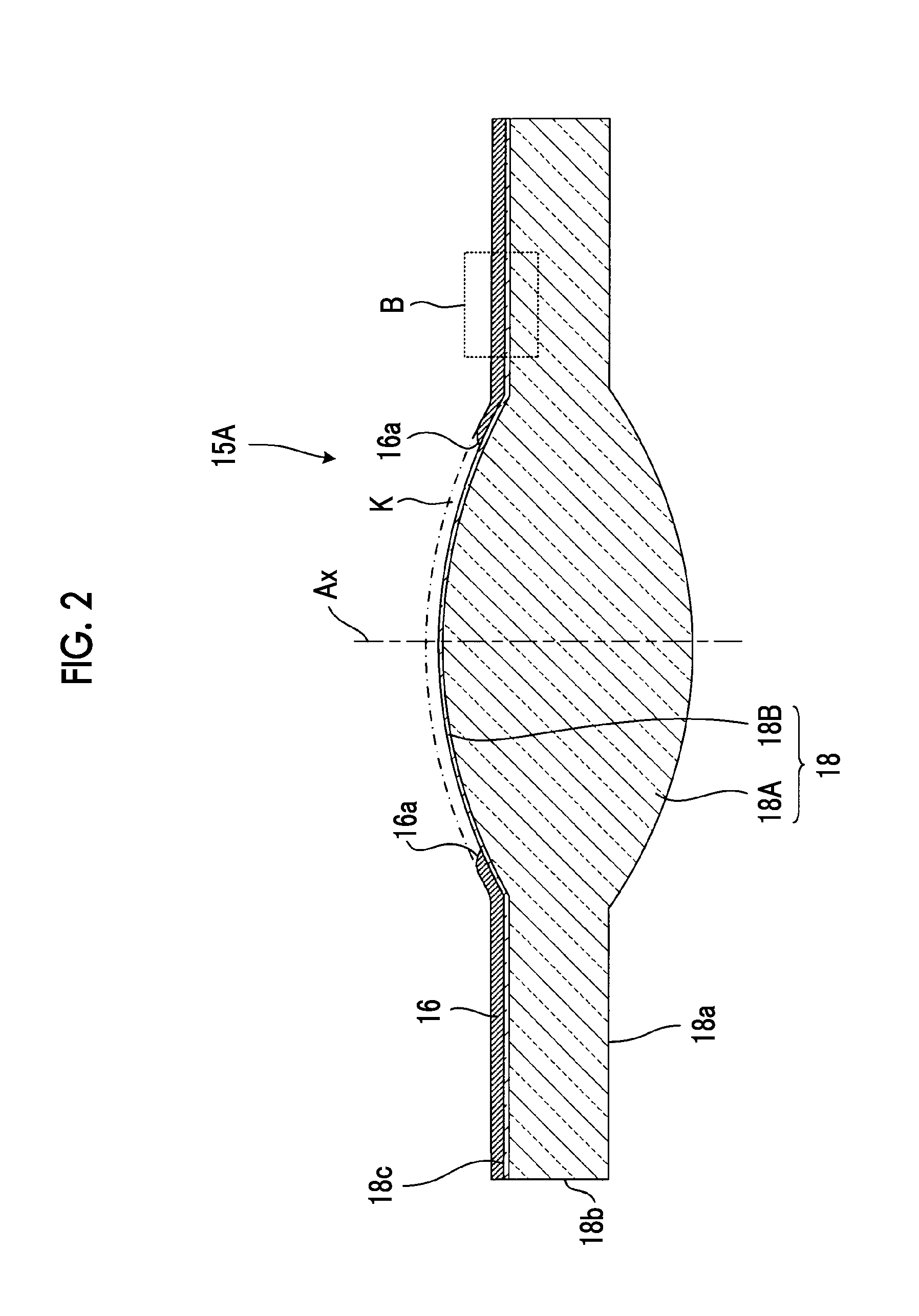
[0045]The lens unit 110 has at least one (five in the example of FIG. 1) optical lens 15 which is disposed to overlap in a direction of a lens optical axis Ax insid...


PUM


Abstract

A method of manufacturing an optical element as defined herein, includes: coating, by an ink jet method, the part of the surface of the optical base member with an ink which contains a light blocking material containing the particles while sequentially shifting, by an interval of T, an area of the surface of the optical base member to be coated with the ink, to form the concave-convex shape of the light blocking layer on the part of the surface of the optical base member.

Description

CROSS REFERENCE TO RELATED APPLICATION[0001]This is a continuation of International Application No. PCT / JP2015 / 056075 filed on Mar. 2, 2015, and claims priority from Japanese Patent Application No. 2014-040561 filed on Mar. 3, 2014, the entire disclosures of which are incorporated herein by reference.BACKGROUND OF THE INVENTION[0002]1. Field of the Invention[0003]The present invention relates to an electronic apparatus such as a digital camera or a mobile phone, an imaging module that is built into and used in the electronic apparatus, an optical element and a lens unit that are mounted on the imaging module, and a method of manufacturing the optical element.[0004]2. Description of the Related Art[0005]In imaging modules which are built into and used in electronic apparatuses such as digital cameras and mobile phones, unnecessary incident light is eliminated such that flare or ghosts are prevented from occurring. In such a manner, the imaging modules have been improved in terms of i...

Claims


Application Information

Patent Timeline
IPC IPC(8): G02B27/00G02B1/10
CPCG02B1/10G02B27/0018G02B5/003G02B5/005G02B13/001
Inventor TAKADA, GOROTANI, TAKEHARUTAKAHASHI, HIROKIKISHINE, YASUNOBU
Owner FUJIFILM CORP
Why Eureka
Try Eureka