Semi conductor device

Inactive Publication Date: 2005-06-16
LAPIS SEMICON CO LTD
View PDF18 Cites 5 Cited by
  • Summary
  • Abstract
  • Description
  • Claims
  • Application Information

AI Technical Summary

Benefits of technology

[0012] In a semiconductor device according to the present invention, a first semiconductor chip comprises a second circuit element region which surrounds a first electrode group and is surrounded by a second electrode group, that is, it comprises a circuit element region directly above which wires electrically connecting the first electrode group and a third electrode group to each other are not present, so that it is possible t

Problems solved by technology

In a semiconductor device described in Patent Document 1, wires for electrically connecting first electrodes and third electrodes to each other are positioned above a first semiconductor chip, and hence circuit elements formed on the first semiconductor chip are subject to an influence of noise generated from the wires, with the result that the reliability of the semiconductor device is liable to deterior

Method used


Image

  • Semi conductor device
  • Semi conductor device

Examples


Example

[0016] The following will describe in detail embodiments of the present invention with reference to drawings. Like components in these drawings are indicated by like reference numerals.

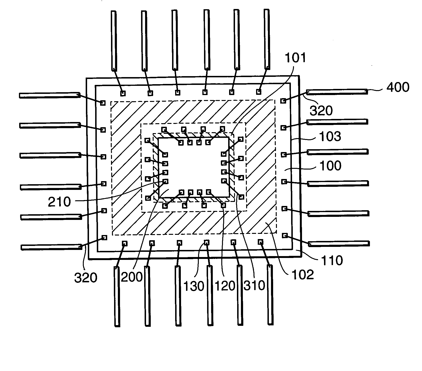
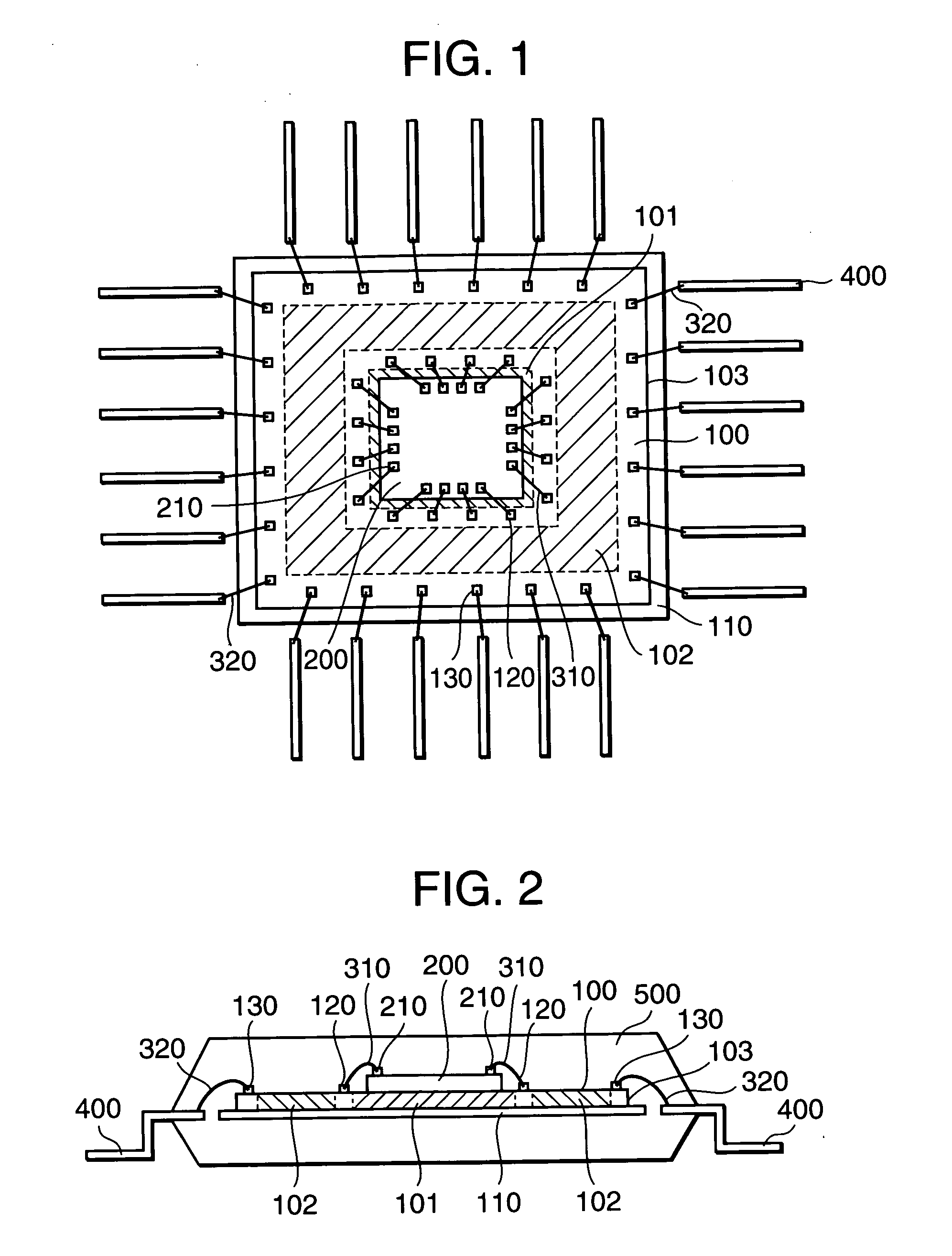
[0017] An embodiment of the present invention is described below with reference to FIGS. 1 and 2. FIG. 1 is a plan view of a semiconductor device related to the present embodiment and FIG. 2, a cross-sectional view of the same semiconductor device.

[0018] As shown in FIGS. 1 and 2, the semiconductor device according to the present embodiment comprises a first semiconductor chip 100 and a second semiconductor chip 200 mounted on the first semiconductor device 100.

[0019] In the present embodiment, the first semiconductor chip 100 is adhered and fixed onto a support 110 with an adhesive agent etc. The first semiconductor chip 100 and the second semiconductor chip 200 each have a substrate made of silicon, on which substrate circuit elements are formed.

[0020] Since the second semiconductor chip 200 is ...


PUM


Abstract

A semiconductor device according to the present invention comprises, on a first semiconductor chip, a first circuit element region in which a first electrode group is arranged along an outer periphery of the first semiconductor chip in such a manner as to surround a second semiconductor chip, a second electrode group is arranged along the outer periphery of the first semiconductor chip in such a manner as to surround the first electrode group, and the first semiconductor chip is surrounded by the first electrode group, and a second circuit element region which surrounds the first electrode group and is surrounded by the second electrode group.

Description

BACKGROUND OF THE INVENTION [0001] 1. Field of the Invention [0002] The present invention relates to a multiple chip package (MCP) type semiconductor device in which a plurality of semiconductor chips are mounted in one package. [0003] 2. Description of the Related Art [0004] In a conventional MCP type semiconductor device, as described in, for example, Patent Document 1, a second semiconductor chip is mounted on a first semiconductor chip. On the first semiconductor chip, first electrodes and second electrodes are formed, and on the second semiconductor chip, third electrodes are formed. [0005] The plurality of first electrodes are provided along an outer periphery of the first semiconductor chip, and the plurality of the second electrodes are arranged between the outer periphery of the first semiconductor chip and the first electrodes and along the outer periphery of the first semiconductor chip. [0006] Furthermore, the first electrodes and the third electrodes are electrically co...

Claims


Application Information

Patent Timeline
IPC IPC(8): H01L25/18H01L21/60H01L23/495H01L25/065H01L25/07
CPCH01L23/49575H01L25/0657H01L24/49H01L24/48H01L2225/06527H01L2225/0651H01L2224/48091H01L2224/48145H01L2224/48247H01L2224/49171H01L2225/06506H01L2924/00014H01L2924/00H01L2224/05554H01L2224/45099H01L2224/45015H01L2924/207H01L2924/00012
Inventor SAEKI, YOSHIHIROHIRATSUKA, SHINJICHABATA, DAIGO
Owner LAPIS SEMICON CO LTD
Why Eureka
Try Eureka