Array substrate for in-plane switching mode liquid crystal display device and method of fabricating the same

a liquid crystal display and substrate technology, applied in optics, instruments, electrical equipment, etc., can solve the problems of color shift dependence, narrow viewing angle, and conventional lcd devices having longitudinal electric fields, so as to improve the aperture ratio, prevent color shift, and increase the viewing angle

Inactive Publication Date: 2005-06-16
LG DISPLAY CO LTD
View PDF6 Cites 43 Cited by
  • Summary
  • Abstract
  • Description
  • Claims
  • Application Information

AI Technical Summary

Benefits of technology

[0021] An advantage of the present invention is to provide an array substrate and a method of forming the array substrate for an IPS-LCD device to increase the viewing angle.
[0022] Another advantage of the present invention is to provide an array substrate and a method of forming the array substrate for an IPS-LCD device to prevent a color shift.
[0023] Another advantage of the present invention is to provide an array substrate and a method of forming the array substrate for an IPS-LCD device to provide a uniform director of liquid crystal molecules in all directions.
[0024] Another advantage of the present invention is to provide an array substrate and a method of forming the array substrate for an IPS-LCD device to improve the aperture ratio.
[0025] Additional features and advantages of the invention will be set forth in the description which follows and in part will be apparent from the description, or may be learned by practice of the invention. These and other advantages of the invention will be realized and attained by the structure particularly pointed out in the written description and claims hereof as well as the appended drawings.
[0026] To achieve these and other advantages, an embodiment in accordance with the principles of the present invention provides an array substrate for use in an in-plane switching liquid crystal display device. The array substrate for an in-plane switching liquid crystal display device includes: a gate line on a substrate; a data line crossing the gate line to define a pixel region; a thin film transistor connected to the gate line and the data line; a common line parallel to and spaced apart from the gate line, a common electrode extending from the common line and including a plurality of common electrode patterns; a pixel connecting line connected to a capacitor electrode; and a pixel electrode extending from the pixel connecting line and including a plurality of pixel electrode patterns, wherein one of the plurality of common electrode patterns and one of the plurality of pixel electrode patterns form concentric rings of pixel and common electrode patterns that are within an open region of another one of the plurality of common electrode patterns.

Problems solved by technology

However, conventional LCD devices having the longitudinal electric field have a drawback in that they have a very narrow viewing angle.
One of the pixel electrodes 56 of the pixel is connected to a drain electrode 62 so that all of the pixel electrodes 56 can electrically communicate with the TFT T. However, the IPS-LCD device having the above-mentioned multi domains has a problem of color shift depending on the viewing angles, because the liquid crystal molecules have long and thin shapes.

Method used


Image

  • Array substrate for in-plane switching mode liquid crystal display device and method of fabricating the same
  • Array substrate for in-plane switching mode liquid crystal display device and method of fabricating the same
  • Array substrate for in-plane switching mode liquid crystal display device and method of fabricating the same

Examples


first embodiment

[0060] In the first embodiment illustrated in FIG. 5, the pixel region “P” has a multi-domain structure including four domains separated by the pixel connecting line 141 and the common line 114. To prevent reduction of a lateral electric field between the first common electrode pattern 120a and the first pixel electrode pattern 138a, the capacitor electrode 140 may be formed to have a smaller area than the first common electrode pattern 120a so as to not overlap a boundary portion of the first common electrode pattern 120a. Moreover, since aperture areas between the common electrode 120 and pixel electrode 138 have a circular structure, the liquid crystal directors become the same in all directions such that the color shift can be prevented. Furthermore, the image quality of the IPS-LCD device is improved, and the IPS-LCD device has much wider viewing angle. Although FIG. 5 shows common electrode 120 including two common electrode patterns 120a and 120b and the pixel electrode 138 i...

second embodiment

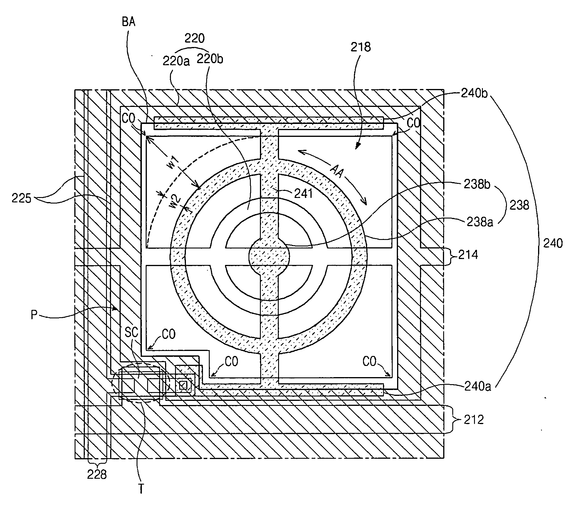
[0061]FIG. 6 is a plan view illustrating an array substrate for an IPS-LCD device according to the present invention. As shown in FIG. 6, a gate line 212 is transversely arranged across the figure and a data line 228 is disposed substantially perpendicular to the gate line 212. The gate line 212 and data line 228 define a pixel region “P” on an array substrate. A semiconductor layer 225 is formed to have a structure corresponding to the data line 228. A thin film transistor (TFT) “T” is connected to the gate line 212 and the data line 228, and the semiconductor layer 225 of the TFT “T” constitutes a semiconductor region “SC.”

[0062] A common electrode 220, including first electrode pattern 220a and second common electrode pattern 220b, is formed in the pixel region “P.” A substantially rectangular shaped open region 218 is formed within the common electrode pattern 220a. A second common electrode pattern 220b has a ring shape and is formed within the substantially rectangular shaped ...

third embodiment

[0075]FIG. 8 is a plan view of an array substrate for an IPS-LCD device according to the present invention. As shown in FIG. 8, a gate line 312 is transversely arranged across the figure and a data line 328 is disposed substantially perpendicular to the gate line 312. The gate line 312 and data line 328 define a pixel region “P” on an array substrate. A semiconductor layer 325 is formed to have a structure corresponding to the data line 328 and a thin film transistor (TFT) “T” is connected to the gate line 312 and the data line 328.

[0076] A common electrode 320 including first common electrode pattern 320 and second common electrode pattern 320b are formed in the pixel region “P.” A substantially rectangular shaped open region 318 is formed within the first common electrode pattern 320a. The second common electrode pattern 320b has a spiral shape and extends from the first common electrode pattern 320a into the substantially rectangular shaped open region 318. The common electrode 3...


PUM

PropertyMeasurementUnit
viewing anglesaaaaaaaaaa

Abstract

An array substrate for an in-plane switching liquid crystal display device includes: a gate line on a substrate; a data line crossing the gate line to define a pixel region; a thin film transistor connected to the gate line and the data line; a common line parallel to and spaced apart from the gate line; a common electrode extending from the common line and including a plurality of common electrode patterns; a pixel connecting line connected to a capacitor electrode; and a pixel electrode extending from the pixel connecting line and including a plurality of pixel electrode patterns, wherein one of the plurality of common electrode patterns and one of the plurality of pixel electrode patterns form concentric rings of pixel and common electrode patterns that are within an open region of another one of the plurality of common electrode patterns.

Description

[0001] This application claims the benefit of Korean Patent Application Nos. 2003-090358 and 2004-0025956, filed on Dec. 11, 2003 and on Apr. 14, 2004, respectively, which is hereby incorporated by reference as if fully set forth herein. BACKGROUND OF THE INVENTION [0002] 1. Field of the Invention [0003] The present invention relates to a liquid crystal display device. More particularly it relates to a liquid crystal display device implemementing in-plane switching (IPS) in which an electric field is generated in a plane that is parallel to the substrate of the device. [0004] 2. Discussion of the Related Art [0005] A liquid crystal display device uses the optical anisotropy and polarization properties of liquid crystal molecules to produce an image. The long thin shapes of the liquid crystal can be aligned to have an orientation in a specific direction. The alignment direction of the liquid crystals can be controlled by an applied electric field. In other words, as an applied electr...

Claims


Application Information

Patent Timeline
Patent Type & Authority Applications(United States)
IPC IPC(8): G02F1/1343G02F1/1362
CPCG02F1/134363G02F2201/40G02F2201/122G02F1/136213
Inventor LEE, YUN-BOK
Owner LG DISPLAY CO LTD
Why Eureka
Try Eureka