Operational transconductance amplifier with DC offset elimination and low mismatch

a transconductance amplifier and operation technology, applied in the field of transconductor, can solve the problems of reducing the restoration function, the inability to eliminate the dc offset generated in the input voltage, and the wrong operation of the system, so as to reduce the mismatch in the transconductor circuit, increase the output resistance, and reduce the mismatch

Active Publication Date: 2005-06-30
ELECTRONICS & TELECOMM RES INST
View PDF7 Cites 29 Cited by
  • Summary
  • Abstract
  • Description
  • Claims
  • Application Information

AI Technical Summary

Benefits of technology

[0013] The present invention provides an operational transconductance amplifier (OTA) capable of eliminating an input DC offset and compensating a mismatch of a signal so that an output DC value can be fixed with maintaining a linear range and a large output resistance value of a conventional transconductor.
[0014] According to an aspect of the present invention, there is provided a transconductor including a common mode control DC offset elimination circuit receiving input / output voltages to stabilize current supplying and output DC value constantly, and a first differential amplifier and a second differential amplifier reducing a mismatch in a transconductor circuit and increasing an output resistance in order to prevent a DC voltage applied to input / output nodes from being saturated or a circuit from wrongly operating due to a DC offset or a mismatch of the circuit.

Problems solved by technology

The DC offset degrades a restoration function of the signal, and causes a wrong operation of the system since it makes an operational point of next stage be a saturation status.
However, in the above case, although the output voltage can be maintained constantly, the DC offset generated in the input voltages vpi1, vmi1, vpi2, and vmi2 cannot be eliminated.
In addition, in a case where a mismatch in the output voltage is generated due to a change of device size after performing processes, the mismatch cannot be eliminated.

Method used


Image

  • Operational transconductance amplifier with DC offset elimination and low mismatch
  • Operational transconductance amplifier with DC offset elimination and low mismatch
  • Operational transconductance amplifier with DC offset elimination and low mismatch

Examples


Embodiment Construction

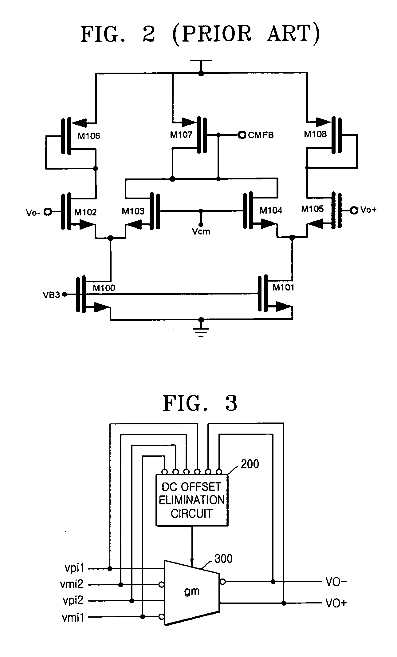
[0025]FIG. 3 is a circuit diagram showing a transconductor according to the present invention.

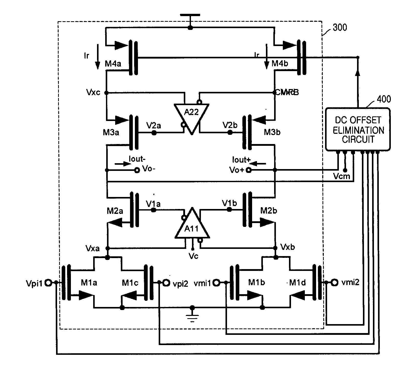
[0026] Referring to FIG. 3, the transconductor of the present invention includes a transconductor circuit 300 and a direct current (DC) offset elimination circuit 400. The transconductor circuit 300 converts input voltages vpi1, vmi1, vpi2, and vmi2 so that the input voltages are in proportion to a transconductance gm, and outputs output voltages vo+ and vo−. The DC offset elimination circuit 400 receives the dual-pair inputs vpi1, vmi1, vpi2, and vmi2, the constant output vo+, and the sub-output vo− to generate DC offset elimination voltage. The DC offset elimination voltage is input into the transconductor circuit 300 so that the affects of the DC offset in the transconductor circuit 300 can be eliminated.

[0027]FIG. 4 is a circuit diagram showing the transconductor of FIG. 3 in more detail.

[0028] Referring to FIG. 4, the transconductor circuit 300 of FIG. 3 includes input transistors M...


PUM


Abstract

Provided is a transconductor capable of eliminating a direct current (DC) offset component of a signal and compensating a mismatch of the signal. The transconductor includes amplifiers of simple circuit structures, and a common mode control DC offset elimination circuit. The transconductor includes a common mode control DC offset elimination circuit unit receiving input / output voltages to stabilize the current supplying and the output DC value, a first amplifier and a second amplifier reducing a mismatch in a transconductor circuit and increasing an output resistance, in order to prevent a signal distortion or a wrong operation of the circuit that is caused by the mismatch signal and unstable DC voltage.

Description

BACKGROUND OF THE INVENTION [0001] This application claims the priority of Korean Patent Application No. 2003-97756, filed on Dec. 26, 2003, in the Korean Intellectual Property Office, the disclosure of which is incorporated herein in its entirety by reference. [0002] 1. Field of the Invention [0003] The present invention relates to a transconductor, and more particularly, to a transconductor, of which direct current (CD) offset component is cancelled and a mismatch characteristic is improved. [0004] 2. Description of the Related Art [0005] An operational transconductance amplifier (OTA) is a current amplifier that amplifies an applied input voltage and outputs the input voltage as an output voltage in proportion to a transconductance (Gm). In a case where the OTA is applied in a communication system of direct conversion type, a signal of high frequency is converted into baseband signal based on a direct current (DC), and a DC offset largely affects the performances of the system. T...

Claims


Application Information

Patent Timeline
Patent Type & Authority Applications(United States)
IPC IPC(8): H03F3/45
CPCH03F3/45188H03F3/45659H03F2203/45574H03F2203/45356H03F2203/45394H03F3/45717H03F3/45
Inventor KIM, YOUNG HOPARK, MUN YANG
Owner ELECTRONICS & TELECOMM RES INST
Why Eureka
Try Eureka