Method of manufacturing CMOS transistor by using SOI substrate

Active Publication Date: 2005-06-30
DONGBU ELECTRONICS CO LTD +1
View PDF3 Cites 3 Cited by
  • Summary
  • Abstract
  • Description
  • Claims
  • Application Information

AI Technical Summary

Benefits of technology

[0014] In order to solve the aforementioned problems, an object of the present invention is to provide a m

Problems solved by technology

However, as recognized by the present inventor, in a CMOS transistor where p-type and n-channel MOS transistors are formed parallel to each other in the same layer in a sin

Method used


Image

  • Method of manufacturing CMOS transistor by using SOI substrate
  • Method of manufacturing CMOS transistor by using SOI substrate
  • Method of manufacturing CMOS transistor by using SOI substrate

Examples


Example

[0024] Now, exemplary embodiments of the present invention will be described with reference to the attached drawings. However, the present invention can be embodied in various modifications and thus is not limited to the embodiments described below.

[0025] FIGS. 6 to 11 are cross sectional views for explaining a CMOS transistor according to embodiments of the present invention.

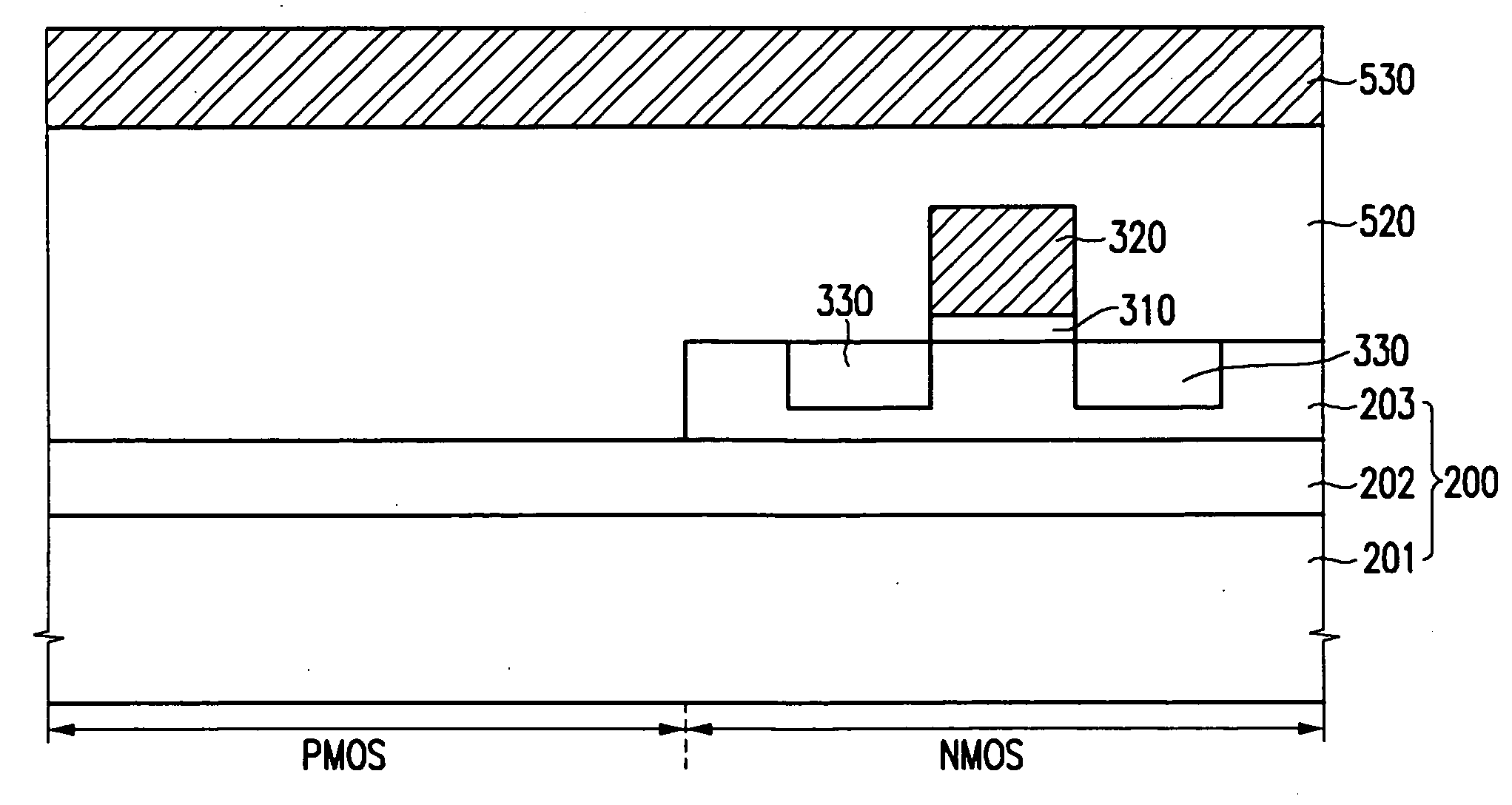
[0026] Referring to FIG. 6, a SOI (silicon on insulator) substrate 200 having an insulating layer 202 between lower and upper silicon layers 201 and 203 is prepared. The insulating layer 203 is typically a buried oxide layer.

[0027] The SOI substrate 200 includes a first region NMOS where an n-channel MOS transistor is to be disposed and a second region PMOS where a p-channel MOS transistor is to be disposed.

[0028] Next, a first gate insulating layer pattern 310 and a first gate conductive layer pattern 320 is subsequently formed on the upper silicon layer 203 of the first region NMOS in the SOI substrate 20...


PUM


Abstract

In a method of manufacturing a CMOS transistor, an n-channel MOS transistor is formed on an upper MOS transistor in a first region of an SOI substrate having first and second regions. Next, an insulating layer of the SOI substrate is exposed by removing an upper silicon layer in a second region, and then, a first insulating layer is formed to cover the first and second regions. Next, a silicon epitaxial layer is formed on the first insulating layer of the second region, and then, a p-channel MOS transistor is formed on the silicon epitaxial layer. An n-channel MOS transistor is formed on the upper silicon layer of the SOI substrate and a p-channel MOS transistor on the first insulating layer has a vertical step (relative to the n-channel MOS transistor), so that it is possible to increase integration degree.

Description

BACKGROUND OF THE INVENTION [0001] 1. Field of the Invention [0002] The present invention relates to a method of manufacturing a MOS transistor, and more particularly, to a method of manufacturing a CMOS transistor by using a SOI (silicon on insulator) substrate to increase integration degree. [0003] 2. Description of the Related Art [0004] FIGS. 1 to 5 are cross sectional views for explaining a method of manufacturing a conventional MOS transistor, such as a p-channel MOS transistor. [0005] Referring to FIG. 1, an active region where a MOS transistor is to be formed is defined by forming an element isolation layer 110 on an n-type semiconductor substrate 100. Alternatively, instead of the n-type semiconductor substrate 100, a p-type semiconductor substrate may be used. In this case, an n-type well region is formed on the p-type semiconductor substrate. [0006] Next, a gate stack is formed by subsequently stacking a gate insulating layer pattern 120 and a gate conductive layer patter...

Claims


Application Information

Patent Timeline
IPC IPC(8): H01L27/092H01L21/8228H01L21/84H01L27/06H01L27/12
CPCH01L27/0688H01L21/84H01L21/8228H01L27/092H01L27/12
Inventor KIM, HAK-DONG
Owner DONGBU ELECTRONICS CO LTD
Why Eureka
Try Eureka