Resistive random access memory

Active Publication Date: 2017-11-16
WINBOND ELECTRONICS CORP
View PDF25 Cites 2 Cited by
  • Summary
  • Abstract
  • Description
  • Claims
  • Application Information

AI Technical Summary

Benefits of technology

[0004]The invention provides a resistive random access memory which can reduce the dimension of

Problems solved by technology

However, as integrated circuits are aiming toward a higher degree of integration through miniaturization, the dimension of the resistive random access memory device need to be reduced in order to increase the degree

Method used


Image

  • Resistive random access memory
  • Resistive random access memory
  • Resistive random access memory

Examples


first embodiment

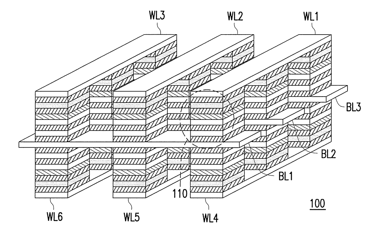
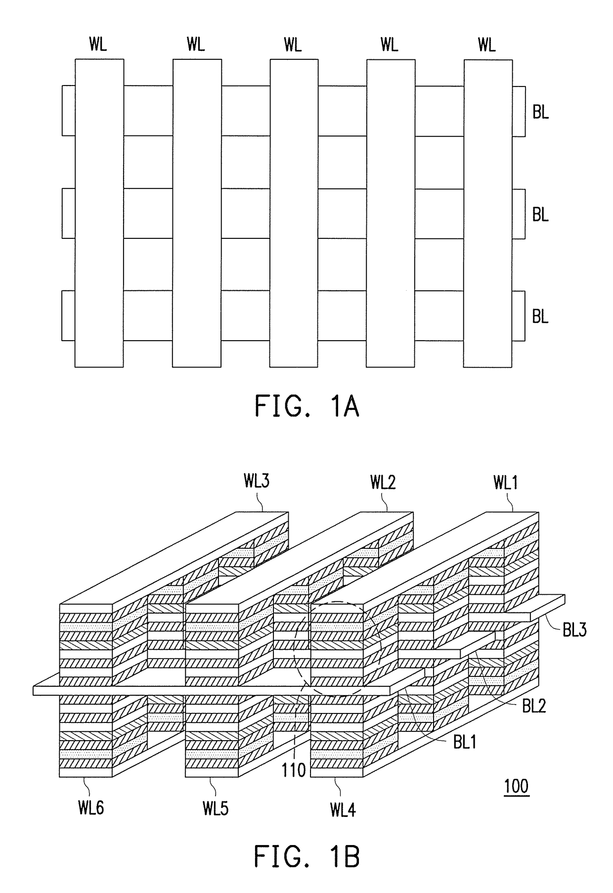
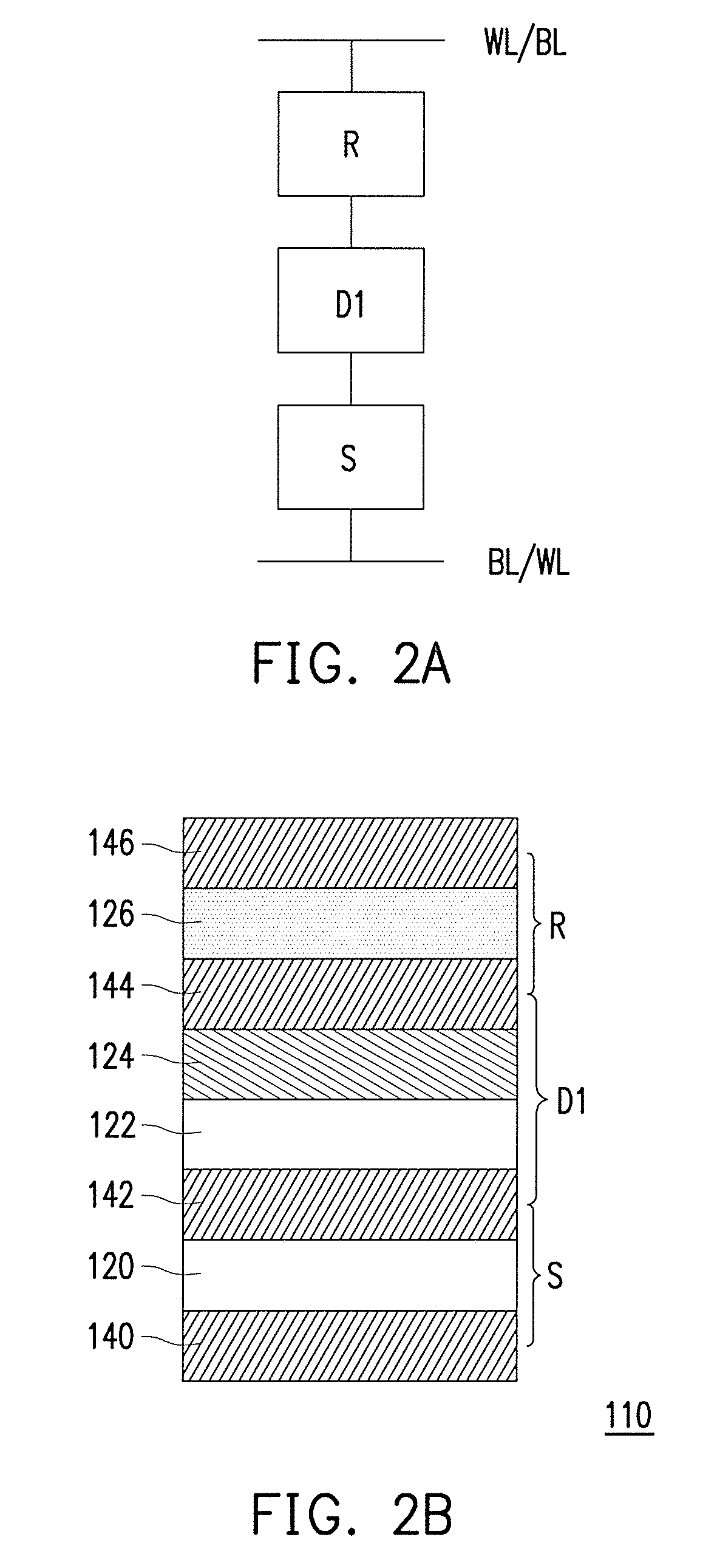
[0054]Referring to FIG. 4A and FIG. 4B, the memory cell 110 includes the selector structure S, the current limiter structure D1, a current limiter structure D2, and the resistor structure R, wherein the current limiter structure D1 is disposed between the selector structure S and the conductive lines WL / BL, the resistor structure R is disposed between the current limiter structure D1 and the conductive lines WL / BL, and the current limiter structure D2 is disposed between the resistor structure R and the conductive lines WL / BL. The layers of each structure and materials of each layer of the selector structure S, the current limiter structure D1, and the resistor structure R are the same as the first embodiment, it will not repeat them.

[0055]The current limiter structure D2 includes a conductive layer 148, a metal layer 130, a current limiting material layer 128, and the conductive layer 146 sequentially. Materials of the conductive layer 148 and the conductive layer 146 are conductiv...

second embodiment

[0059]Referring to FIG. 5A and FIG. 5B, the memory cell 110 includes the selector structure S, the current limiter structure D1, the current limiter structure D2, and the resistor structure R, wherein the current limiter structure D1 is disposed between the selector structure S and the conductive lines WL / BL, the resistor structure R is disposed between the selector structure S and the conductive lines BL / WL, and the current limiter structure D2 is disposed between the resistor structure R and the conductive lines BL / WL. The layers of each structure and materials of each layer of the selector structure S, the current limiter structure D1, and the resistor structure R are the same as the second embodiment, it will not repeat them.

[0060]The current limiter structure D2 includes the conductive layer 150, the metal layer 130, the current limiting material layer 128, and a conductive layer 158 sequentially. Materials of the conductive layer 150 and the conductive layer 158 are conductive...


PUM


Abstract

A resistive random access memory includes a memory cell disposed at an intersection point between a first conductive line and a second conductive line. The memory cell includes a selector structure, a first current limiter structure and a resistor structure. The first current limiter structure is disposed between the selector structure and the first conductive line. The resistor structure is disposed between the selector structure and the second conductive line or between the first current limiter structure and the first conductive line.

Description

BACKGROUND OF THE INVENTIONField of the Invention[0001]The invention relates to a non-volatile memory, and particularly relates to a resistive random access memory.Description of Related Art[0002]A resistive random access memory (RRAM) belongs to a non-volatile memory. Since the resistive random access memory has advantages such as simple structure, low operating voltage, fast operating time, multi-bit memorization, low cost, good durability, and the like, it is widely studied now. A common basic structure of the resistive random access memory is composed of a transistor and a resistor (1T1R). A resistance value of the resistor is changed by a method of changing the plus bias voltage, so that the device is in a high resistance state or low resistance state, thereby interpreting the digital signals, such as 0 or 1.[0003]However, as integrated circuits are aiming toward a higher degree of integration through miniaturization, the dimension of the resistive random access memory device n...

Claims


Application Information

Patent Timeline
IPC IPC(8): H01L27/24H01L45/00H01L23/528
CPCH01L27/2481H01L23/528H01L45/1246H01L27/2409H01L45/08H01L45/1253H01L45/146H01L45/1233H10B63/20H10B63/84H10N70/20H10N70/828H10N70/826H10N70/8416H10N70/8833H10N70/883H10N70/8836
Inventor CHEN, FREDERICK
Owner WINBOND ELECTRONICS CORP
Why Eureka
Try Eureka