

Method for patterning a material layer with desired dimensions
- Summary
- Abstract
- Description
- Claims
- Application Information
AI Technical Summary
Benefits of technology
Problems solved by technology
Method used
Image

Examples
Embodiment Construction
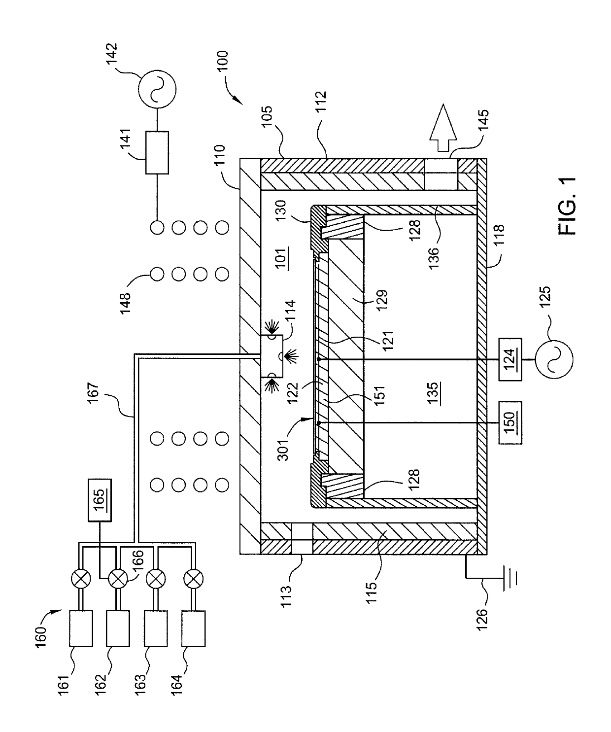
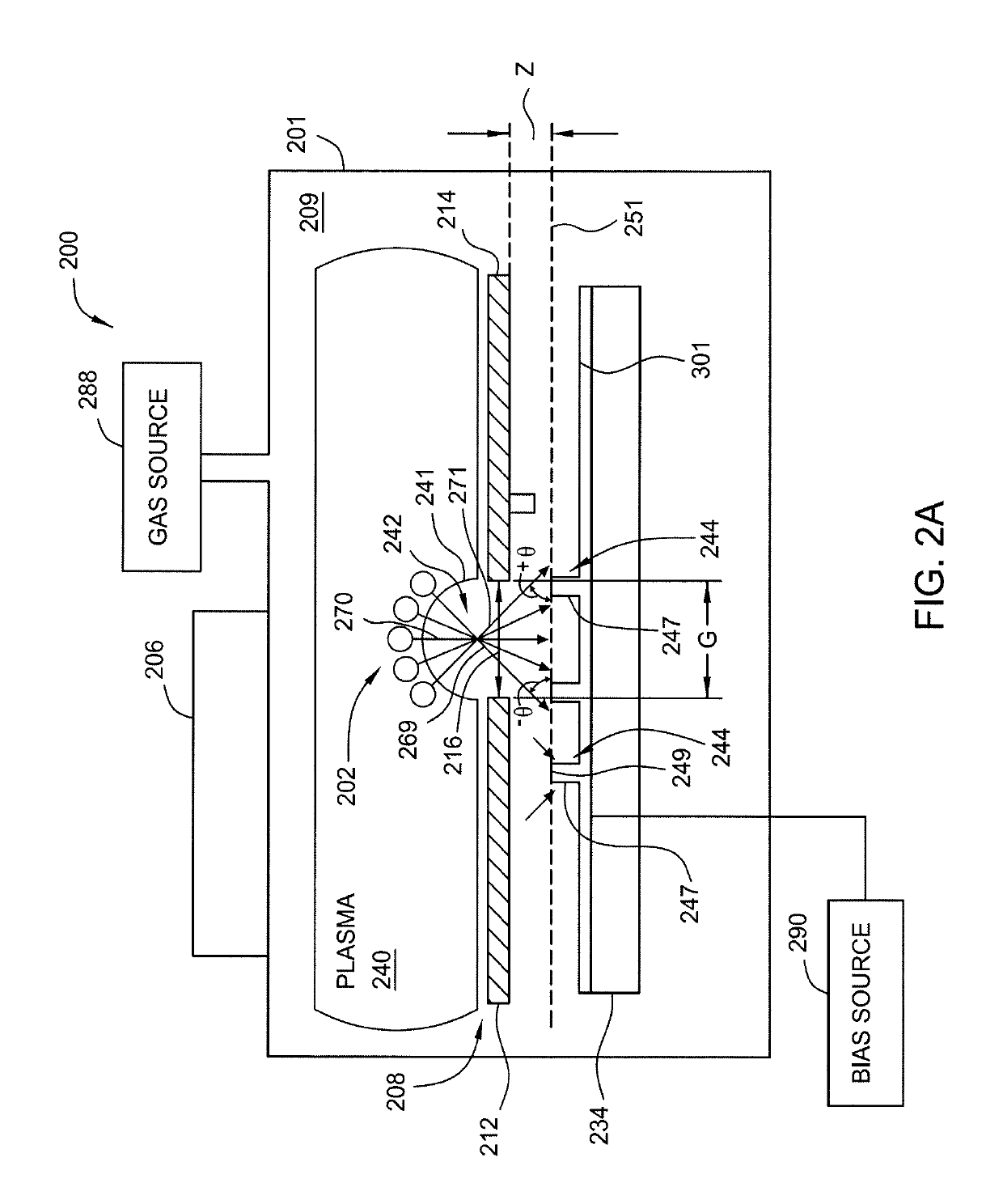
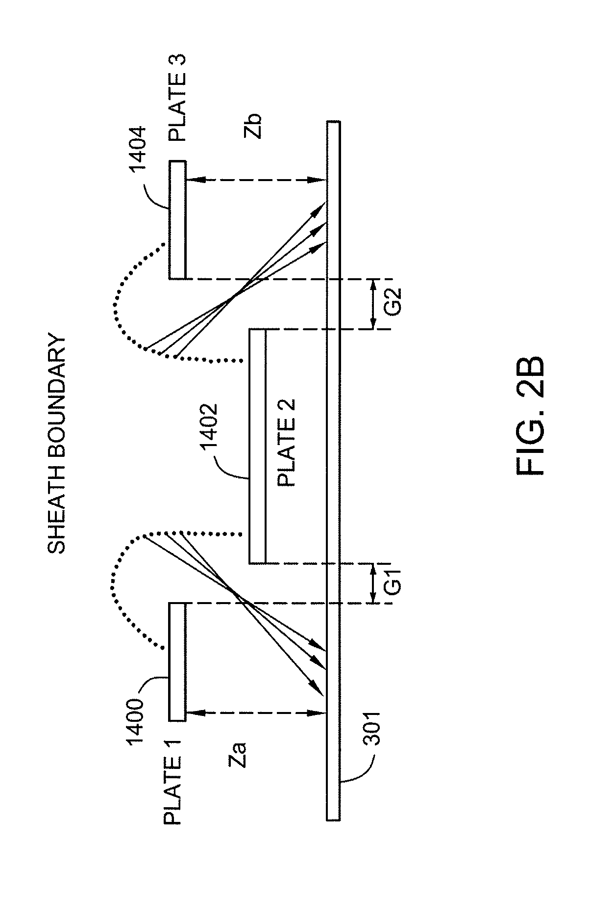
[0025]Methods for patterning features and manufacturing nanostructures with desired small dimensions in a film stack are provided. The methods utilize a directional etching process to pattern material layers in the film stack layer at a desired angle, so as to laterally or directionally etch the material layers as needed. By doing so, an etching rate may be altered or modified while etching the features in the material layer in the film stack with different feature densities so as to improve etching selectivity and enhance feature transfer dimension and profile control.
[0026]The term “substrate” as used herein refers to a layer of material that serves as a basis for subsequent processing operations and includes a surface to be cleaned. For example, the substrate can include one or more material containing silicon containing materials, IV group or III-V group containing compounds, such as Si, polysilicon, amorphous silicon, Ge, SiGe, GaAs, InP, InAs, GaAs, GaP, InGaAs, InGaAsP, GaSb,...
PUM
 Abstract
Description
Claims
Application Information