

Circuit board structure and method for fabricating the same
- Summary
- Abstract
- Description
- Claims
- Application Information
AI Technical Summary
Benefits of technology
Problems solved by technology
Method used
Image

Examples
Embodiment Construction
[0022] The following illustrative embodiments are provided to illustrate the disclosure of the present invention, these and other advantages and effects can be apparently understood by those in the art after reading the disclosure of this specification. The present invention can also be performed or applied by other different embodiments. The details of the specification may be on the basis of different points and applications, and numerous modifications and variations can be devised without departing from the spirit of the present invention.
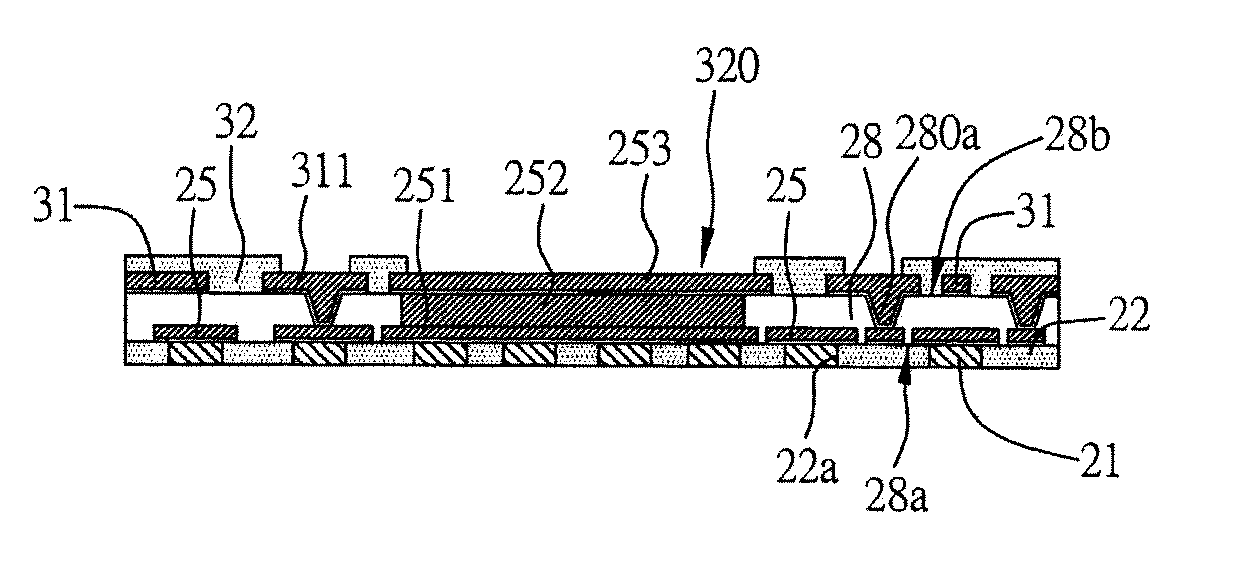
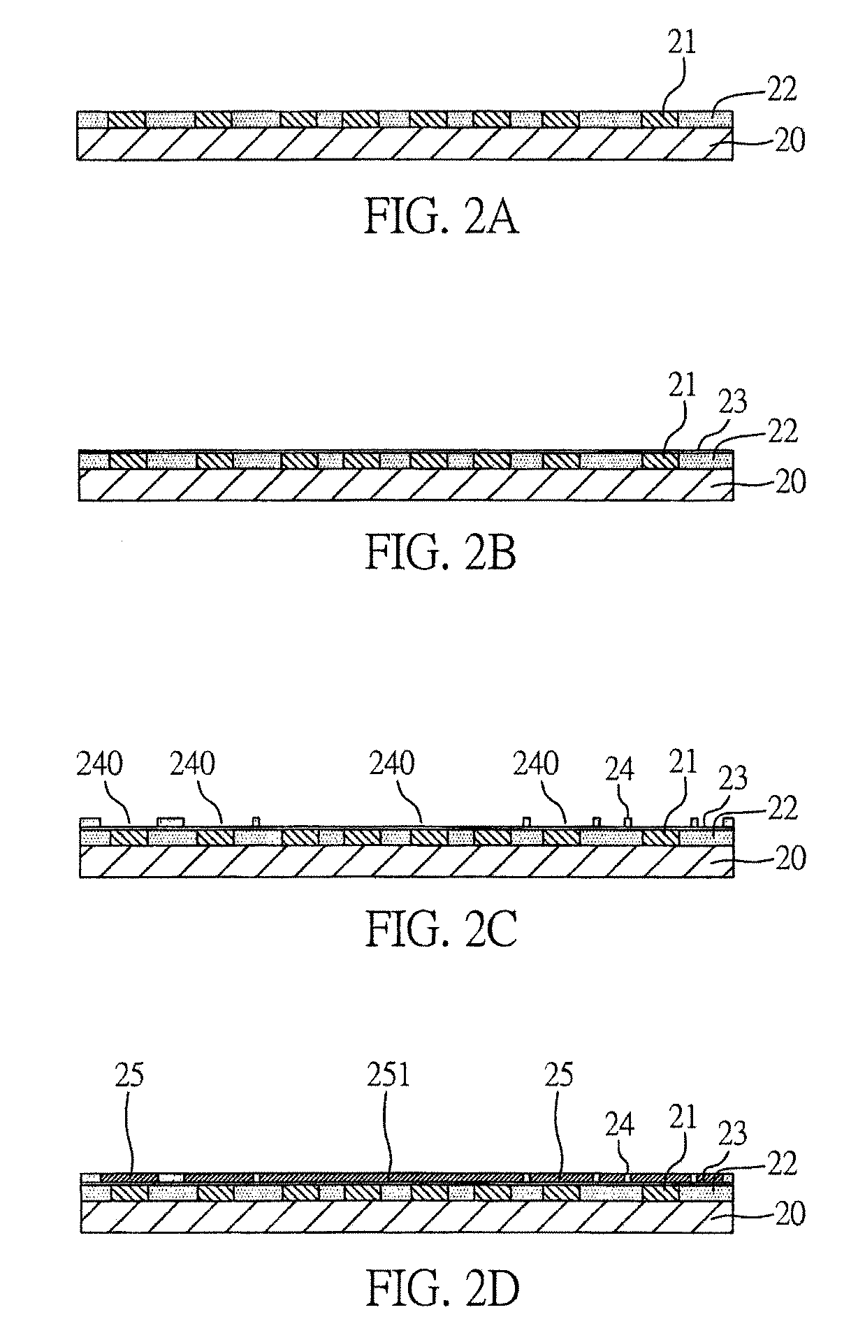
[0023]FIGS. 2A to 2J are ten cross sectional views demonstrating a method for fabricating a circuit board structure of a first embodiment according to the present invention.
[0024] As shown in FIG. 2A, the method comprises providing a carrier board 20, and forming a plurality of conductive bumps 21 on the carrier board 20 by first forming on the carrier board 20 a resistive layer having a plurality of openings for exposure of the carrier board ...
PUM
 Abstract
Description
Claims
Application Information