Sacrificial inorganic polymer intermetal dielectric damascene wire and via liner

a dielectric damascene and inorganic polymer technology, applied in the direction of semiconductor devices, semiconductor device details, electrical apparatus, etc., can solve the problems of low mechanical strength, easy cracking, and lack of mechanical rigidity, and achieve the effect of thermal mechanical stress

Active Publication Date: 2005-07-14
AURIGA INNOVATIONS INC
View PDF19 Cites 43 Cited by
  • Summary
  • Abstract
  • Description
  • Claims
  • Application Information

AI Technical Summary

Benefits of technology

[0029] More specifically, the mechanically rigid dielectric may comprise SiO2, SiCOH, or F-doped glass and have a thickness that typically ranges from about 100 nm to about 1,000 nm, preferably being 300 nm. The mechanically rigid dielectric may comprise a coefficient of thermal expansion ranging from about 0.1 ppm / ° C. to about 5.0 ppm / ° C. The coefficient of thermal expansion of the mechanically rigid dielectric may be substantially matched to the coefficient of thermal expansion of the via metal. By reducing the differential in the coefficient of thermal expansion between the via metal and the mechanical rigid dielectric, the thermal mechanical stresses that may be produced at the interface of the via and the mechanical rigid dielectric are reduced.

Problems solved by technology

The main problem with low-k materials is that they lack mechanical rigidity and easily crack when subjected to thermal and mechanical stresses.
Despite the ability of low-k materials to reduce the interconnect capacitance, forming via interconnects through low-k interlayer dielectrics having low mechanical strength produces a number of disadvantageous results.
For example, if the dielectric is bent or is mechanically stressed, the interconnect metal may break within the via.
Additionally, differences between the thermal coefficient of expansion of the metal interconnect and low-k interlevel and / or intralevel dielectrics produce further stresses that contribute to via breakage and chip failure.
Attempts to overcome the above disadvantages have resulted in further difficulties.
Therefore, introducing refractory metal within the via opening 24 disadvantageously increases the resistance of the interconnect structure 10.
Additionally, refractory metals, such as Ta, are difficult to deposit using chemical vapor deposition.

Method used


Image

  • Sacrificial inorganic polymer intermetal dielectric damascene wire and via liner
  • Sacrificial inorganic polymer intermetal dielectric damascene wire and via liner
  • Sacrificial inorganic polymer intermetal dielectric damascene wire and via liner

Examples


Embodiment Construction

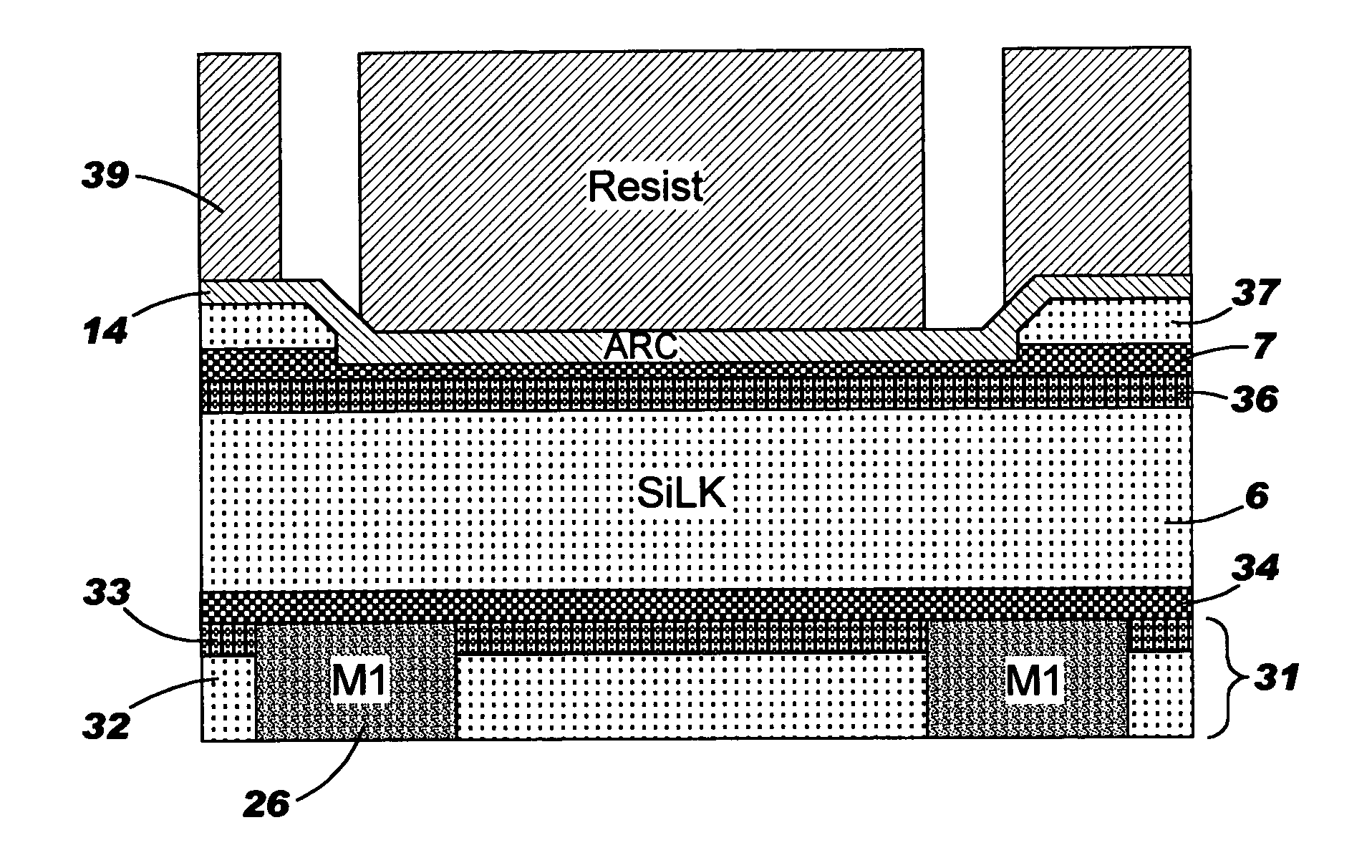
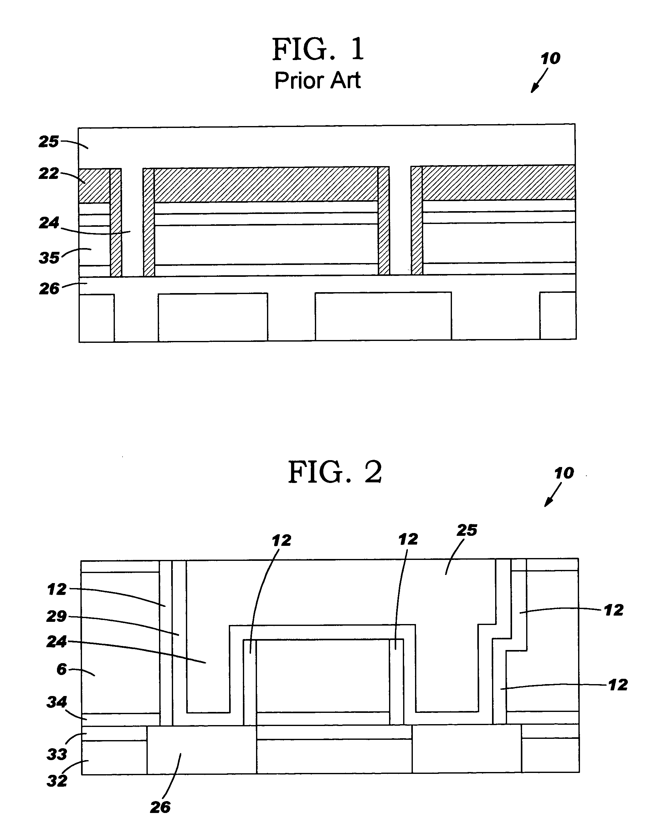
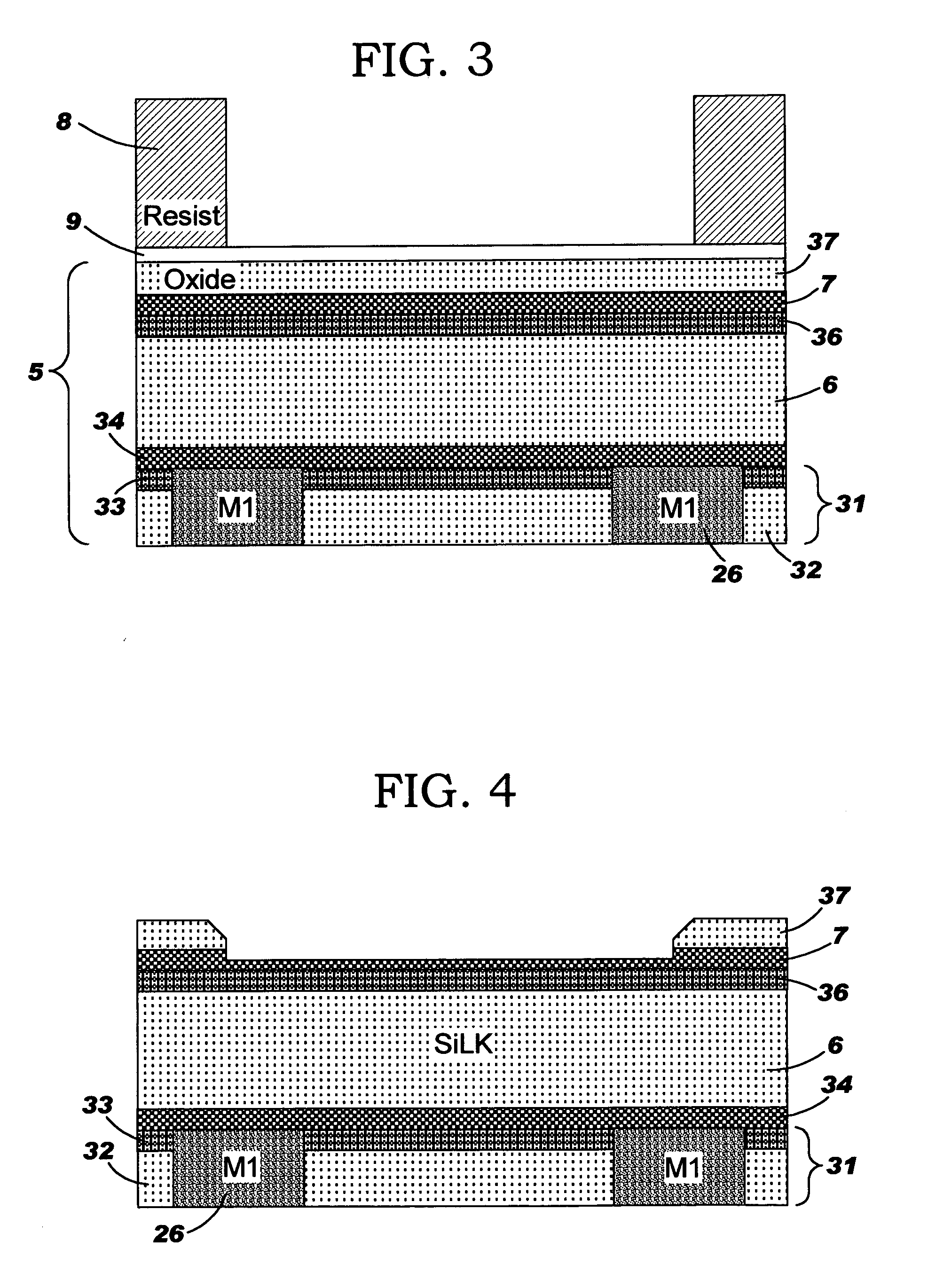
[0040] An interconnect structure, and method of forming thereof, will now be discussed in greater detail referring to the drawings accompanying the present invention. It is noted in the accompanying drawings like and corresponding elements are referred to by like reference numbers. Although the drawings show the presence of two wiring layers, the present invention is not limited to low resistance interconnect structures having only two wiring layers. Instead, the present invention works equally well with interconnect structure having a plurality of wiring levels, one over the other, in which a liner material enhances the rigidity of low-k dielectrics.

[0041] The present invention provides low resistance via interconnects through rigid low-k interlevel and intralevel dielectric layers. In one embodiment of the present invention, the rigidity of low-k dielectric layers in the interconnect structures is increased by a thin mechanically rigid liner lining the sidewall of a via opening i...


PUM

PropertyMeasurementUnit
dielectric constantaaaaaaaaaa
thicknessaaaaaaaaaa
thicknessaaaaaaaaaa

Abstract

The present invention provides a method of forming a rigid interconnect structure, and the device therefrom, including the steps of providing a lower metal wiring layer having first metal lines positioned within a lower low-k dielectric; depositing an upper low-k dielectric atop the lower metal wiring layer; etching at least one portion of the upper low-k dielectric to provide at least one via to the first metal lines; forming rigid dielectric sidewall spacers in at least one via of the upper low-k dielectric; and forming second metal lines in at least one portion of the upper low-k dielectric. The rigid dielectric sidewall spacers may comprise of SiCH, SiC, SiNH, SiN, or SiO2. Alternatively, the via region of the interconnect structure may be strengthened with a mechanically rigid dielectric comprising SiO2, SiCOH, or doped silicate glass.

Description

BACKGROUND OF INVENTION [0001] 1. Field of the Invention [0002] The present invention relates generally to the manufacture of semiconductor devices, and more particularly to a method of forming an interconnect via through a low dielectric constant (k) dielectric material. [0003] 2. Background of the Invention [0004] In the production of microelectronic devices, integrated circuits utilize multilevel wiring structures for interconnecting regions within devices and for interconnecting one or more devices within integrated circuits. Conventionally, forming interconnect structures begins with forming a lower level of wiring followed by the deposition of an interlevel dielectric layer and then a second level of wiring, where the first and second wiring levels may be connected by one or more metal filled vias. [0005] Conventional interconnect structures employ one or more metal layers. Each metal layer is typically made from aluminum alloys or tungsten. Interlevel and intralevel dielectri...

Claims


Application Information

Patent Timeline
Patent Type & Authority Applications(United States)
IPC IPC(8): H01L21/312H01L21/314H01L21/316H01L21/768H01L23/522H01L23/532
CPCH01L21/312H01L21/3121H01L2924/0002H01L21/3122H01L21/3148H01L21/31612H01L21/76807H01L21/76811H01L21/76813H01L21/76831H01L21/76835H01L23/5226H01L23/53238H01L23/5329H01L23/53295H01L2221/1063H01L2924/3011H01L2924/00H01L21/0217H01L21/02164H01L21/02167H01L21/02266H01L21/02274H01L21/02271H01L21/02126H01L21/02118
Inventor GAMBINO, JEFFREY P.STAMPER, ANTHONY K.
Owner AURIGA INNOVATIONS INC
Why Eureka
Try Eureka