Light-emitting device having reflecting layer formed under electrode

a technology of light-emitting devices and electrodes, which is applied in the direction of semiconductor devices, basic electric elements, electrical equipment, etc., can solve the problems of low illumination efficiency and achieve the effect of high illumination efficiency

Inactive Publication Date: 2005-07-21
EPISTAR CORP
View PDF4 Cites 26 Cited by
  • Summary
  • Abstract
  • Description
  • Claims
  • Application Information

AI Technical Summary

Benefits of technology

[0008] It is therefore a primary objective of the present invention to provide a light-emitting diode with high illumination efficiency to solve the above-mentioned problem. The light-emitting diode has a reflecting layer located under the metal electrodes to avoid light being absorbed.

Problems solved by technology

However, when operating the above-mentioned light-emitting diodes, the p-type and n-type electrodes will absorb light from the active layer and lower the illumination efficiency.

Method used


Image

  • Light-emitting device having reflecting layer formed under electrode
  • Light-emitting device having reflecting layer formed under electrode
  • Light-emitting device having reflecting layer formed under electrode

Examples


first embodiment

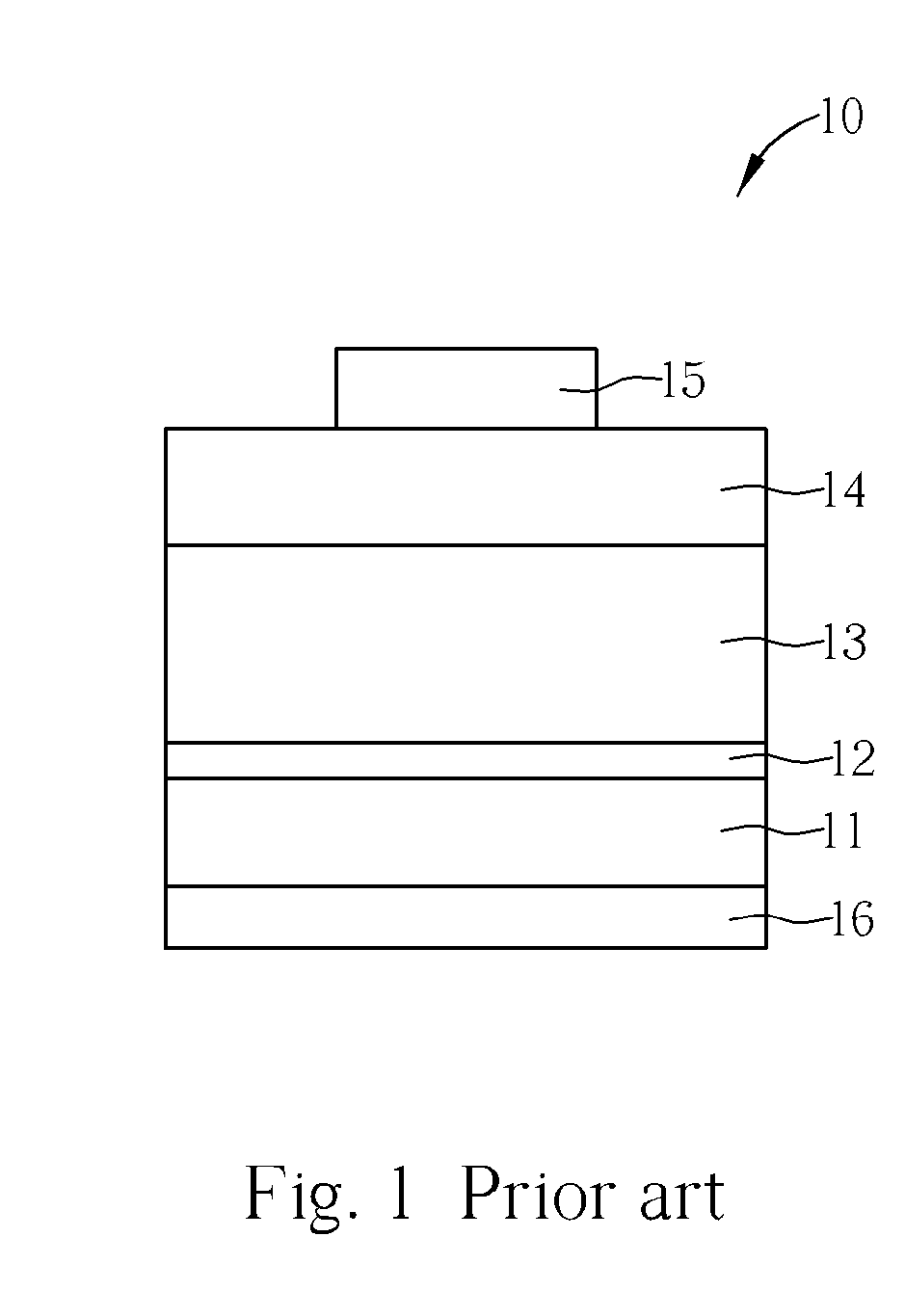
[0020] Please refer to FIG. 3, which is a structural diagram of the present invention. A light-emitting diode 30 comprises a substrate 31, a distributed Bragg reflector (DBR) 32, an active layer 33, a p-type semiconductor layer 34, a p-type electrode 35, an n-type electrode 36, and a reflecting layer 38. The fabrication process of the light-emitting diode 30 is firstly forming the DBR 32, the active layer 33, and the p-type semiconductor layer 34 on the substrate 31. Then the reflecting layer 38 is formed on portion of the p-type semiconductor layer 34. Finally, the p-type electrode 35 is formed on the reflecting layer 38, and the n-type electrode 36 is formed on the other surface of the substrate 31.

[0021] The substrate 31 is a conductive material, such as n-type GaAs or GaN, and the DBR 32 is composed of multi-layered reflective structures, such as AlAs and GaAs, for reflecting light. The structure of the active layer 33 is homostructure, single heterostructure, double heterostruc...

second embodiment

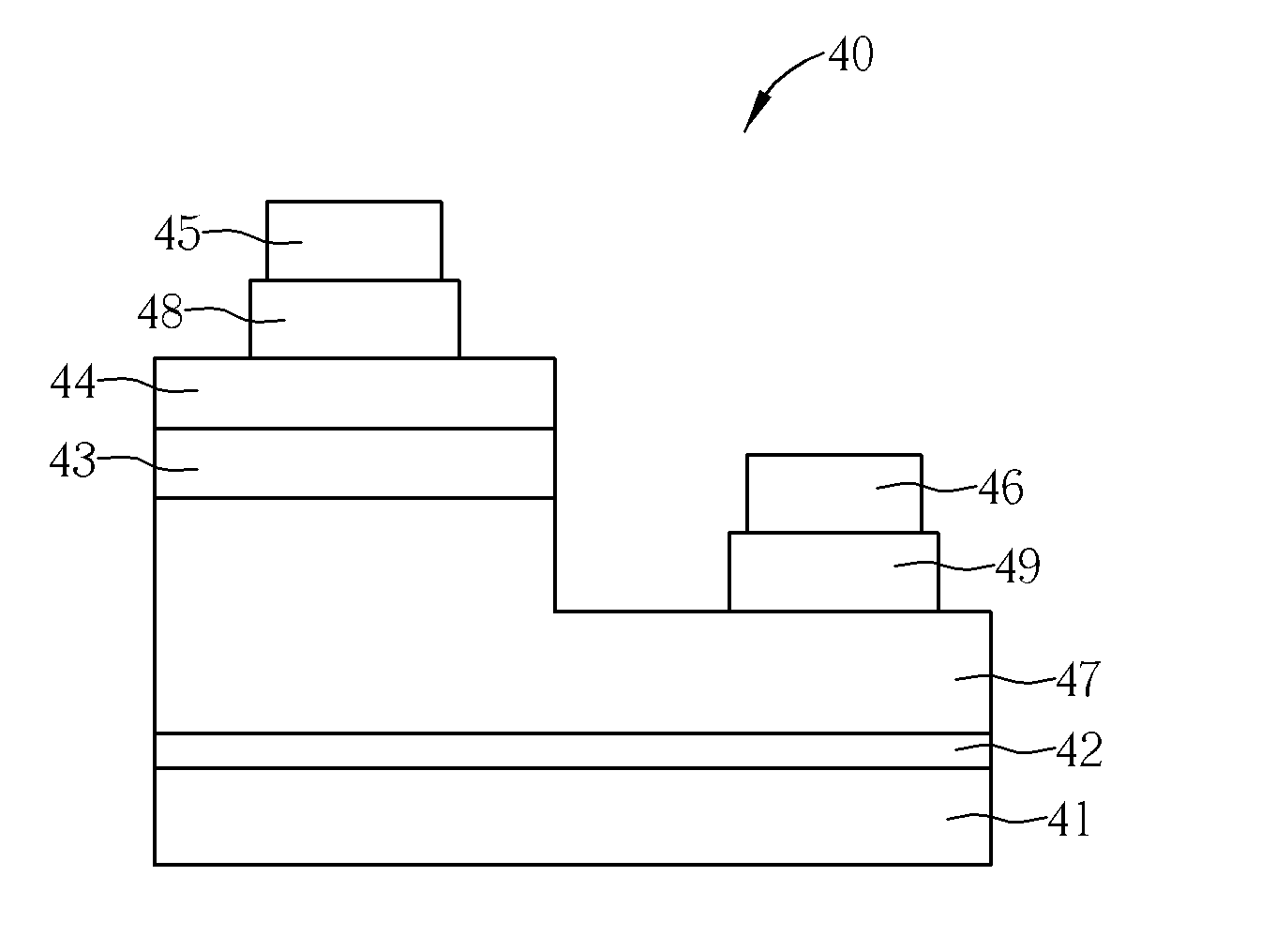
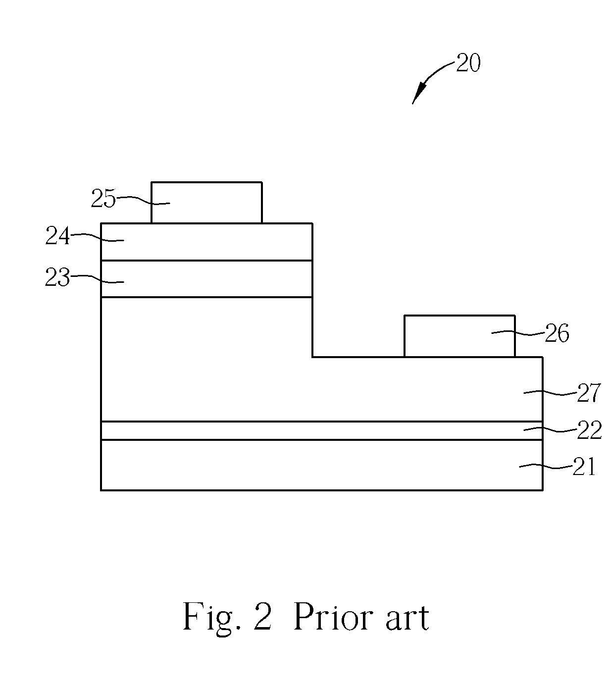
[0023] Please refer to FIG. 4, which is a structural diagram of the present invention. As FIG. 4 shows, a light-emitting diode 40 comprises a substrate 41, a distributed Bragg reflector (DBR) 42, an active layer 43, a p-type semiconductor layer 44, a p-type electrode 45, an n-type electrode 46, an n-type semiconductor layer 47, a first reflecting layer 48, and a second reflecting layer 49. The fabrication process of the light-emitting diode 40 is firstly forming the DBR 42, the n-type semiconductor layer 47, the active layer 43, and the p-type semiconductor layer 44 on the substrate 41. Then an etching process is performed on portion of the p-type semiconductor layer 44 and the active layer 43 to expose portion of the n-type semiconductor layer 47. After that, the first reflecting layer 48 and the p-type electrode 45 are formed on the un-etched p-type semiconductor layer 44, and the second reflecting layer 49 and the n-type electrode 46 are formed on the exposed n-type semiconductor...


PUM


Abstract

The present invention discloses a light-emitting device that has a substrate, an n-type electrode, an active layer, a p-type semiconductor layer, a reflecting layer, and a p-type electrode. The n-type electrode is located on the bottom surface of the substrate and the active layer is located on a top surface of the substrate. The p-type semiconductor layer covers the active layer. The reflecting layer is located on the p-type semiconductor layer and covered by the p-type electrode and has an area not less than the area of the p-type electrode and not more than a half of the area of the p-type semiconductor layer. The reflecting layer is a conductive layer with high reflectivity, and is formed under the p-type electrode to reflect light from the active layer, avoiding light of the light-emitting device being absorbed by the metal electrode.

Description

CROSS REFERENCE TO RELATED APPLICATIONS [0001] This is a continuation-in-part of U.S. application Ser. No. 10 / 605,539, which was filed on Oct. 6, 2003 and is included herein by reference.BACKGROUND OF INVENTION [0002] 1. Field of the Invention [0003] The invention relates to a semiconductor light-emitting device, and more particularly, to a light-emitting diode with high illumination efficiency. [0004] 2. Description of the Prior Art [0005]FIG. 1 is a structural diagram of a light-emitting diode according to the prior art. As FIG. 1 shows, the light-emitting diode 10 comprises a substrate 11, a distributed Bragg reflector (DBR) 12, an active layer 13, a p-type semiconductor layer 14, a p-type electrode 15, and an n-type electrode 16 located under the substrate 11. The substrate 11 is an n-type GaAs substrate, and the DBR 12 is composed of multi-layered reflective structures for reflecting light. The active layer 13 is composed of an n-type AlGaInP lower cladding layer, an AlGaInP ac...

Claims


Application Information

Patent Timeline
Patent Type & Authority Applications(United States)
IPC IPC(8): H01L29/06H01L33/04H01L33/10H01L33/40
CPCH01L33/04H01L33/405H01L33/105
Inventor TSAI, TZONG-LIANGCHANG, CHIH-SUNGCHIEN, WEI-ENCHEN, TZER-PERNG
Owner EPISTAR CORP
Why Eureka
Try Eureka