Manufacturing method of optoelectronic semiconductor device

a manufacturing method and technology of optoelectronic semiconductors, applied in the field of semiconductor devices, can solve the problems of increasing the difficulty of selecting the material of temporary substrates, obstructing the following huge amount of transferring, and limited temporary fixing force, so as to increase the illumination efficiency of manufactured optoelectronic semiconductor devices

Active Publication Date: 2019-09-12
LG DISPLAY CO LTD
View PDF0 Cites 1 Cited by
  • Summary
  • Abstract
  • Description
  • Claims
  • Application Information

AI Technical Summary

Benefits of technology

[0013]As mentioned above, the manufacturing method of an optoelectronic semiconductor device of this disclosure is to form a protective layer to cover the entire micro-sized optoelectronic semiconductor elements, and then to remove the residuals on the back surface of the micro-sized optoelectronic semiconductor element and a part of the micro-sized optoelectronic semiconductor element to expose a new surface of the micro-sized optoelectronic semiconductor element, which is away from the matrix substrate. Accordingly, the residuals remained on the back surface as well as the bu

Problems solved by technology

However, this temporary fixing force must be limited, otherwise it will obstruct the following huge amount transferring of the Micro LEDs.
These requir

Method used


Image

  • Manufacturing method of optoelectronic semiconductor device
  • Manufacturing method of optoelectronic semiconductor device
  • Manufacturing method of optoelectronic semiconductor device

Examples


Embodiment Construction

[0019]The present disclosure will be apparent from the following detailed description, which proceeds with reference to the accompanying drawings, wherein the same references relate to the same elements.

[0020]The “optoelectronic semiconductor device” of this disclosure can be applied to display panels, advertising billboards, sensing devices, backlight modules or lighting devices. If the optoelectronic semiconductor device is a display device, it can be a monochrome or full color display device.

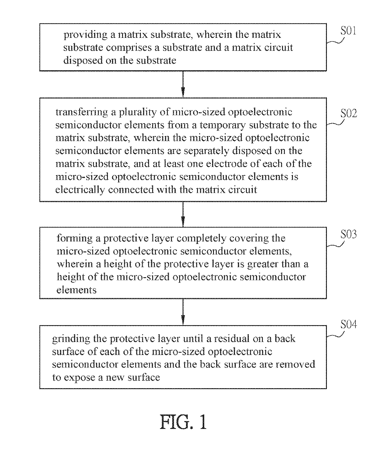
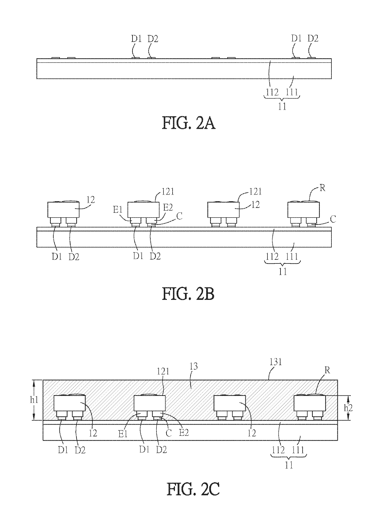
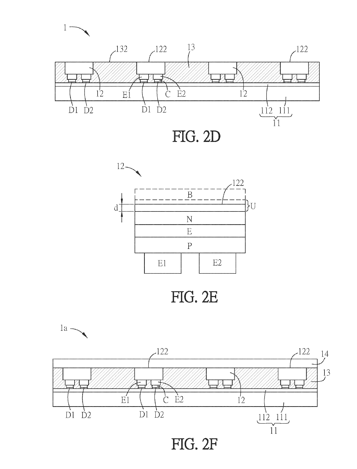
[0021]FIG. 1 is a flow chart of a manufacturing method of an optoelectronic semiconductor device according to an embodiment of this disclosure. As shown in FIG. 1, the manufacturing method of an optoelectronic semiconductor device comprises: providing a matrix substrate, wherein the matrix substrate comprises a substrate and a matrix circuit disposed on the substrate (step S01); transferring a plurality of micro-sized optoelectronic semiconductor elements from a temporary substrate to the mat...


PUM


Abstract

A manufacturing method of an optoelectronic semiconductor device includes: providing a matrix substrate, which comprises a substrate and a matrix circuit disposed on the substrate; transferring a plurality of micro-sized optoelectronic semiconductor elements from a temporary substrate to the matrix substrate, wherein the micro-sized optoelectronic semiconductor elements are separately disposed on the matrix substrate, and at least one electrode of each micro-sized optoelectronic semiconductor element is electrically connected with the matrix circuit; forming a protective layer completely covering the micro-sized optoelectronic semiconductor elements, wherein the height of the protective layer is greater than the height of the micro-sized optoelectronic semiconductor elements; and grinding the protective layer until a residual on a back surface of each micro-sized optoelectronic semiconductor element and the back surface are removed to expose a new surface.

Description

CROSS REFERENCE TO RELATED APPLICATIONS[0001]This Non-provisional application claims priority under 35 U.S.C. § 119(a) on Patent Application No(s). 107107726 filed in Taiwan, Republic of China on Mar. 7, 2018, the entire contents of which are hereby incorporated by reference.BACKGROUNDTechnology Field[0002]The present disclosure relates to a semiconductor device and, in particular, to an optoelectronic semiconductor device and a manufacturing method thereof.Description of Related Art[0003]A GaN-based light-emitting diode is epitaxial on, for example, a sapphire substrate. In the manufacturing process of an optoelectronic semiconductor device, in order to remove the sapphire substrate, the epitaxial wafer is permanently fixed to, for example, a silicon substrate by metal bonding, and then a laser lift-off (LLO) process for the sapphire substrate is performed. The LLO process is to dissociate the gallium nitride at the interface between the gallium nitride layer and the sapphire subst...

Claims


Application Information

Patent Timeline
IPC IPC(8): H01L33/00H01L27/15H01L33/52
CPCH01L33/007H01L27/153H01L2933/005H01L33/0095H01L2933/0033H01L33/52H01L21/02096H01L33/005H01L25/0753
Inventor CHEN, HSIEN-TE
Owner LG DISPLAY CO LTD
Why Eureka
Try Eureka