Semiconductor light emitting device and its manufacturing method

Inactive Publication Date: 2005-08-02
SAMSUNG ELECTRONICS CO LTD
View PDF13 Cites 80 Cited by
  • Summary
  • Abstract
  • Description
  • Claims
  • Application Information

AI Technical Summary

Benefits of technology

[0017]First, according to the invention, because of the embossment formed on the light emitting surface of the semiconductor light emitting device or on the reflecting interface, the external quantum efficiency of the light released from an active layer can be improved significantly.
[0018]Additionally, according to the invention, by making a high concentration of a p-type dopant such as magnesium (Mg) near the surface of a p-type GaN layer, it is possible to ensure ohmic contact with a p-side electrode, reduce the operation voltage of the device, alleviate heat generation and improve the reliability.
[0019]Further, according to the invention, by removing a doping metal layer from the surface of the p-type GaN layer after introducing a p-type dopant like magnesium, exfoliation of the p-side electrode can be prevented. That is, deterioration of the characteristics caused by exfoliation of the electrode can be overcome, and the reliability of the light emitting device can be improved. Simultaneously, by removing the doping metal layer, transparency of the

Problems solved by technology

However, conventional nitride compound semiconductor light emitting devices as shown in FIG. 14 involved problems, namely, high contact resistance at electrode portions and insufficient external quantum efficiency of light.
That is, since GaN has a band gap as wide as 3.4 eV, it is difficult to ensure its ohmic contact with electrodes.
This invites the problems that the contact resistance increases in el

Method used


Image

  • Semiconductor light emitting device and its manufacturing method
  • Semiconductor light emitting device and its manufacturing method
  • Semiconductor light emitting device and its manufacturing method

Examples


Embodiment Construction

[0039]Some embodiments of the invention are explained below with reference to the drawings.

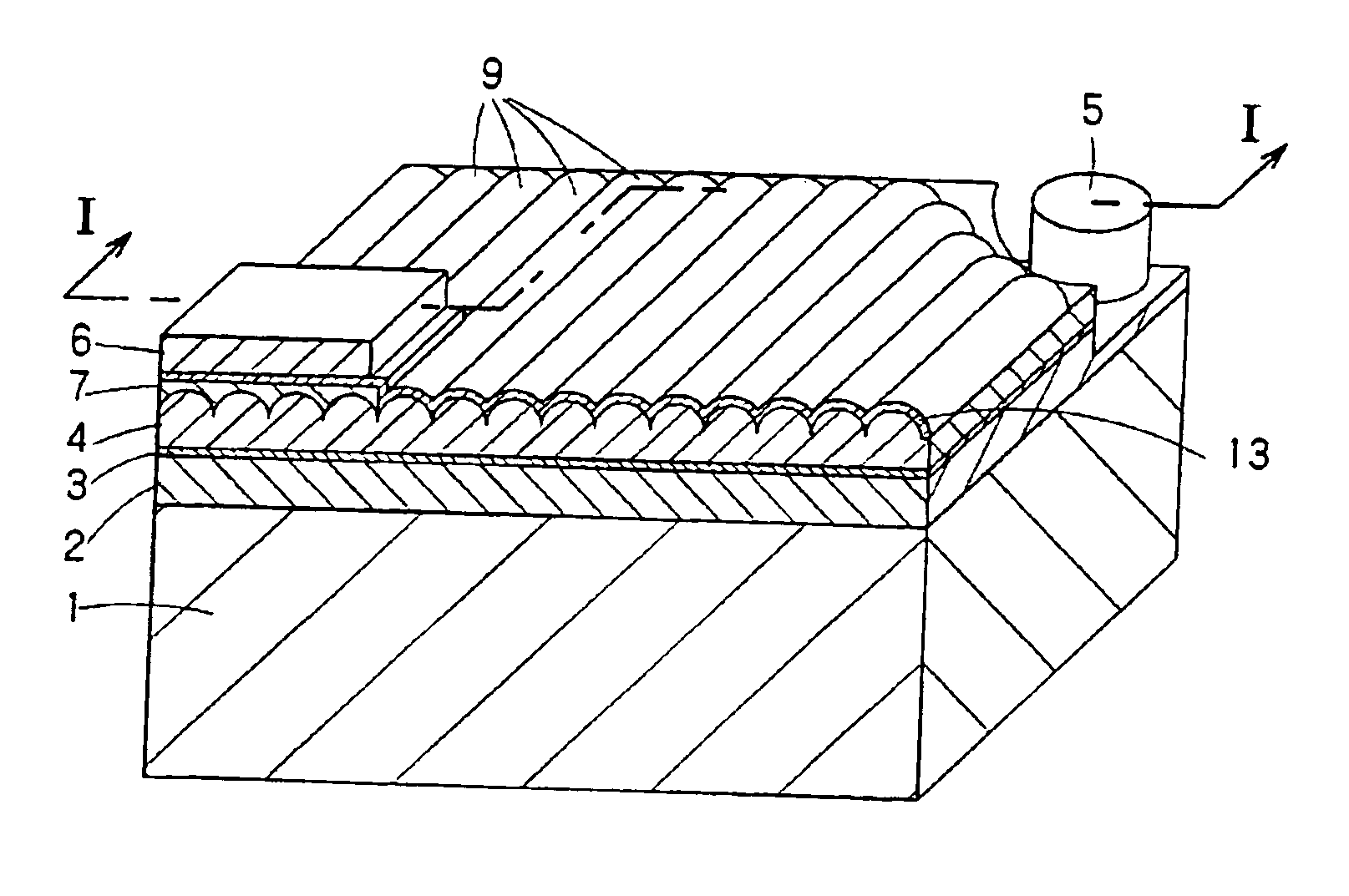
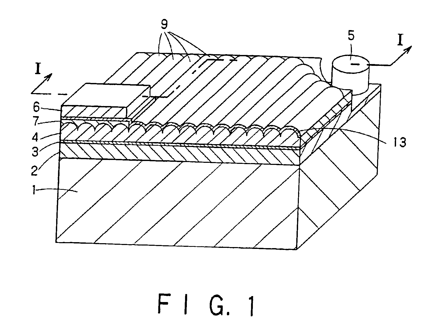
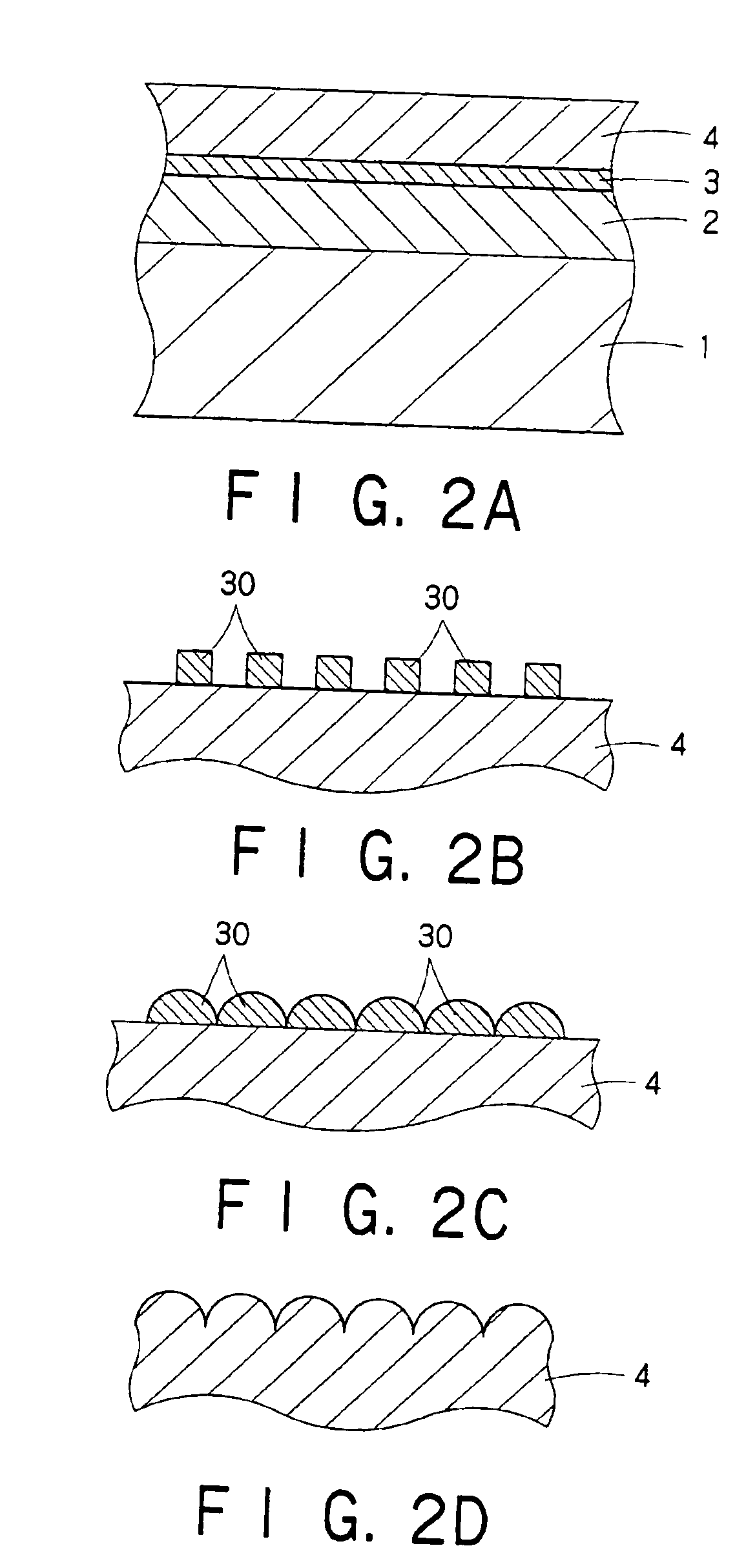
[0040]FIG. 1 is a perspective conceptional diagram illustrating a semiconductor light emitting device according to the invention. The semiconductor light emitting device shown here has a structure sequentially stacking a GaN buffer layer (not shown), n-type GaN layer 2, InGaN light emitting layer 3, and p-type GaN layer 4 on a sapphire substrate 1. The InGaN light emitting layer 3 and the p-type GaN layer 4 are selectively removed by etching to expose the n-type GaN layer 2. Locally formed on the p-type GaN layer 4 is an insulating film 7 for blocking current. Formed on the p-type GaN layer 4 and the insulating film 7 is a p-side transparent electrode 13, and selectively stacked thereon is a p-side bonding pad 6. Further formed on the n-type GaN layer 2 is an n-side electrode 5.

[0041]One of features of the invention lies in embossment formed on the surface of the p-type GaN layer 4. That is, i...


PUM


Abstract

Efficiency of leading out light released from an active layer, i.e. the external quantum efficiency, can be improved remarkably by processing a light lead-out surface to have an embossment. A layer containing a p-type dopant like magnesium (Mg) is deposited near the surface of a p-type GaN layer to diffuse it there, and a p-side electrode is made on the p-type GaN layer after removing the deposited layer. This results in ensuring ohmic contact with the p-side electrode, preventing exfoliation of the electrode and improving the reliability.

Description

[0001]This is a divisional of application Ser. No. 09 / 469,340 filed Dec. 20, 1999 now U.S. Pat. No. 6,495,862 which application is hereby incorporated by reference in its entirety.BACKGROUND OF THE INVENTION[0002]This invention relates to a semiconductor light emitting device and its manufacturing method. More particularly, the invention relates to a light emitting device having a stacked nitride compound semiconductor layer of GaN, InGaN, GaAlN, or the like, which remarkably reduces the operation voltage of the device, increases the luminance, and improves the reliability, and a manufacturing method for manufacturing such a device.[0003]Light emitting devices for wavelength bands from ultraviolet to green or blue are being brought into practice by using nitride compound semiconductors represented by gallium nitride.[0004]In this application, “nitride compound semiconductors” involve III-V compound semiconductors expressed as BxInyAlzGa(1−x−y−z)N (0≦x≦1, 0≦y≦1, 0≦z≦1), and further i...

Claims


Application Information

Patent Timeline
IPC IPC(8): H01L33/00H01L33/20H01L33/22H01L33/32H01L33/38H01L33/42H01L33/48H01L33/50
CPCH01L33/20H01L21/42H01L33/22H01L33/32H01L33/382H01L33/42H01L33/508H01L2933/0016
Inventor OKAZAKI, HARUHIKONITTA, KOICHINOZAKI, CHIHARU
Owner SAMSUNG ELECTRONICS CO LTD
Why Eureka
Try Eureka