Light emitting device and manufacturing method thereof

a technology of light emitting device and manufacturing method, which is applied in the direction of semiconductor/solid-state device manufacturing, semiconductor/conductor device, electrical apparatus, etc., can solve the problems of low energy conversion efficiency (optical output/input power), low emission efficiency of conventional leds having emission wavelengths suitable, and insufficient illumination intensity

Active Publication Date: 2004-04-01
FUJIFILM HLDG CORP +1
View PDF2 Cites 73 Cited by
  • Summary
  • Abstract
  • Description
  • Claims
  • Application Information

AI Technical Summary

Problems solved by technology

However, the emission efficiencies (optical output/current) of the conventional LEDs having emission wavelengths suitable for fixing thermal color-forming layers for yellow and magenta are low, and energy conversion efficiencies (optical output/input power) are also low.
Therefore, the intensities of illumination are too small.
However, when the packaging density is high, it is difficult to sufficiently dissipate heat generate...

Method used


Image

  • Light emitting device and manufacturing method thereof
  • Light emitting device and manufacturing method thereof
  • Light emitting device and manufacturing method thereof

Examples


first embodiment

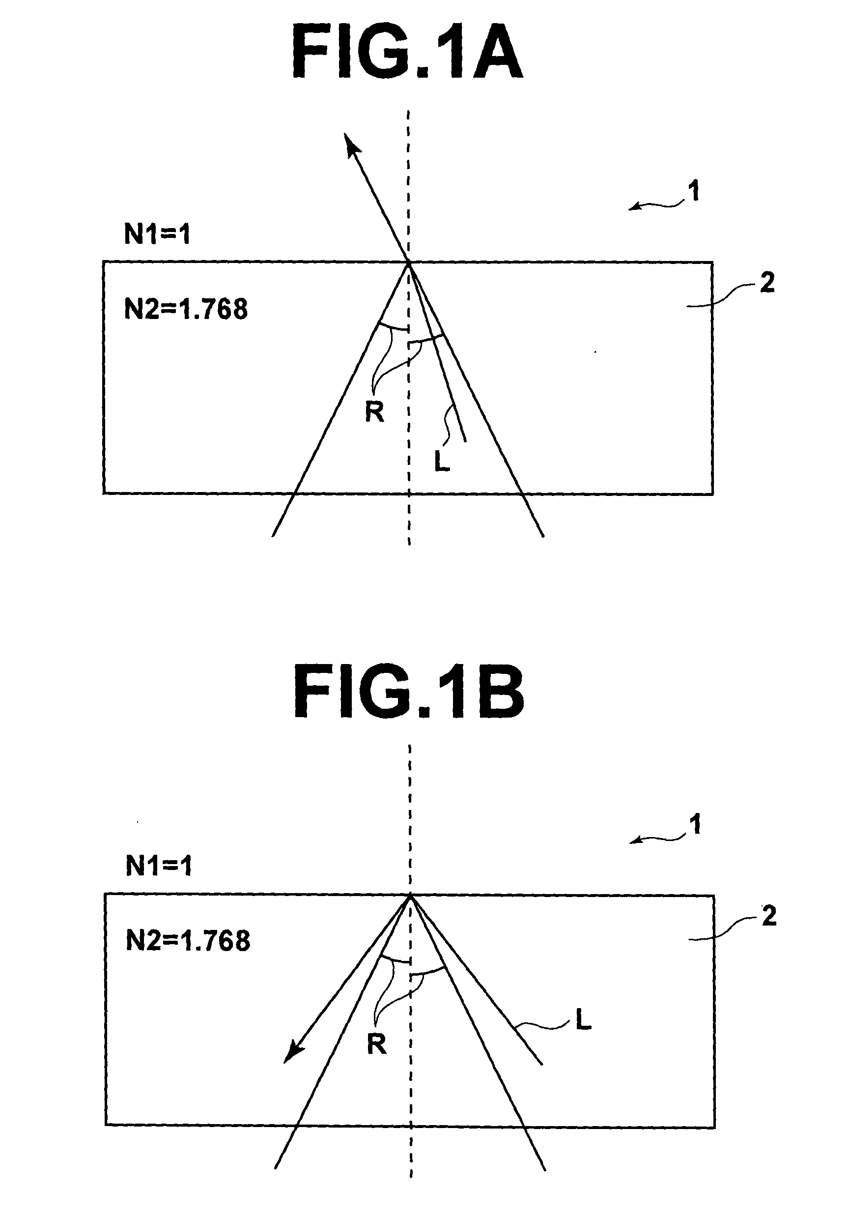
[0047] Before the explanation of the first embodiment of the present invention, the critical angle and reflection of light will be explained.

[0048] FIGS. 1A and 1B are diagrams for explaining the critical angle and reflection of light. In FIGS. 1A and 1B, it is assumed that a piece of sapphire glass 2 is placed in a space filled with air 1. The optical refractive index N1 of the air 1 is one (i.e., N1=1), and the optical refractive index N2 of the sapphire glass 2 is 1.768 (i.e., N2=1.768) At a boundary surface between mediums having different optical refractive indexes, a critical angle R is determined based on the refractive indexes. When light L is incident on the boundary surface at an incident angle not greater than the critical angle R, the light L passes through the boundary surface as illustrated in FIG. 1A. When light L is incident on the boundary surface at an incident angle greater than the critical angle R, the light L is totally reflected at the boundary surface as illu...

second embodiment

[0065] The second embodiment of the present invention will be explained below.

[0066] FIG. 11 is a schematic perspective view of a light emitting device as the second embodiment of the second aspect of the present invention.

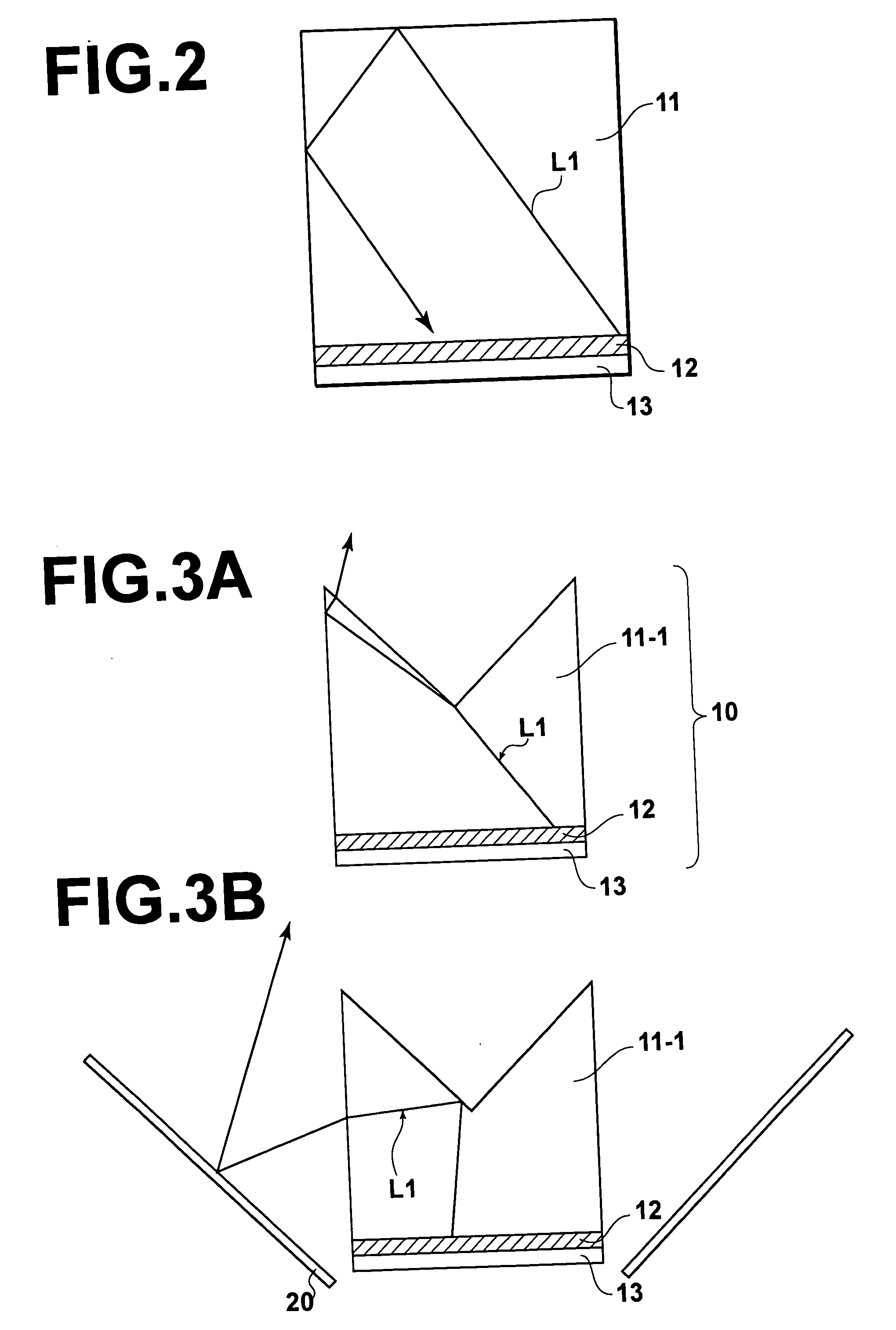
[0067] In the light emitting device 10 according to the first embodiment illustrated in FIGS. 3A and 3B, the upper surface of the sapphire substrate 11-1 per se has a shape containing a portion inclined with respect to the upper surface of the stack of GaN-based compound semiconductor layers 12. On the other hand, in the light emitting device 30 as the second embodiment illustrated in FIG. 11, an optical element 14 is arranged in contact with the upper surface of the sapphire substrate 11-3, and the upper surface (light-exit surface) of the optical element 14 has a quadrangular pyramidal concave shape as the aforementioned shape containing a surface inclined with respect to the upper surface of the stack of GaN-based compound semiconductor layers 12. The optical e...


PUM


Abstract

In a light emitting device, a light emitting element which includes a transparent substrate and a stack of GaN-based compound semiconductor layers formed on the first surface of the transparent substrate is mounted on a lead frame or a printed circuit board so that the transparent substrate is located on the side of the stack of GaN-based compound semiconductor layers opposite to the lead frame or the printed circuit board. The second surface of the transparent substrate opposite to the first surface contains a portion inclined with respect to the first surface. Alternatively, an optical member is arranged in contact with the second surface of the transparent substrate, where a surface of the optical member located on the opposite side to the transparent substrate contains a portion inclined with respect to the first surface of the transparent substrate.

Description

[0001] 1. Field of the Invention[0002] The present invention relates to a light emitting device containing a light emitting element and a process for producing such a light emitting device, where the light emitting element is constituted by a transparent substrate and a stack of GaN-based compound semiconductor layers formed on the transparent substrate.[0003] 2. Description of the Related Art[0004] Conventionally, light emitting devices for light irradiation are used in various apparatuses (e.g., optical reading apparatuses such as facsimile apparatuses and image scanners, and fixing devices in color thermal printers). Various light emitting devices which use light emitting diodes (LEDs) as light sources have been proposed. The LEDs are small in size and relatively stable.[0005] For example, in the fixing devices in color thermal printers, ultraviolet light is applied to thermal color-forming layers in color thermal recording sheets in order to fix recording images thermally record...

Claims


Application Information

Patent Timeline
IPC IPC(8): H01L33/32H01L33/60H01L33/62
CPCH01L33/20H01L33/52H01L2224/16H01L33/62H01L33/58H01L2224/05001H01L2224/05023H01L2224/0508H01L2224/05568H01L2224/05573H01L2224/0603H01L2224/06102H01L2224/1703H01L2924/00014H01L2224/05599H01L2224/05099
Inventor MIZUYOSHI, AKIRA
Owner FUJIFILM HLDG CORP
Why Eureka
Try Eureka